...
The Trenz Electronic TE0xxxTEF1002-xx 02 ... is an industrial-grade ... module ... based on Xilinx ...
...
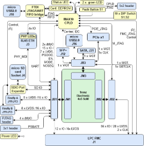
Carrier for 4x5 modules
LPC FMC
- SFP+ connector
- PCIe x1
- SATA connector with power pin 7 configuration for SATADom
- RJ45 Gigabit Ethernet connector
- micro-usb to JTAG/UART bridge
- 2x 8 lane high speed LVDS connectors (firefly)
- micro usb connector
- micro SD card connector
- 4x LED (2User, Power and Status)
- Module reset button
- 10x configuration/user dip switch
MAX10 CPLD
...
| Scroll Title |
|---|
| anchor | Figure_OV_BD |
|---|
| title | TEF1002 block diagram |
|---|
|
| Scroll Ignore |
|---|
| draw.io Diagram |
|---|
| border | false |
|---|
| viewerToolbar | true |
|---|
| |
|---|
| fitWindow | false |
|---|
| diagramName | BD_TEF1002-01 |
|---|
| simpleViewer | false |
|---|
| links | auto |
|---|
| tbstyle | top |
|---|
| lbox | true |
|---|
| diagramWidth | 633 |
|---|
| revision | 48 |
|---|
|
|
| Scroll Only |
|---|
|
|
Main Components
...
| Scroll Title |
|---|
| anchor | Figure_OV_MC |
|---|
| title | TEF1002 main components |
|---|
|
| Scroll Ignore |
|---|
| draw.io Diagram |
|---|
| border | false |
|---|
| viewerToolbar | true |
|---|
| |
|---|
| fitWindow | false |
|---|
| diagramName | TE1002-01_Main_components_top |
|---|
| simpleViewer | false |
|---|
| links | auto |
|---|
| tbstyle | top |
|---|
| lbox | true |
|---|
| diagramWidth | 641636 |
|---|
| revision | 58 |
|---|
|
| draw.io Diagram |
|---|
| border | true |
|---|
| viewerToolbar | true |
|---|
| |
|---|
| fitWindow | false |
|---|
| diagramName | TE1002-01_Main_components_bottom |
|---|
| simpleViewer | false |
|---|
| diagramWidth | 635 |
|---|
| revision | 47 |
|---|
|
|
| Scroll Only |
|---|
|
|
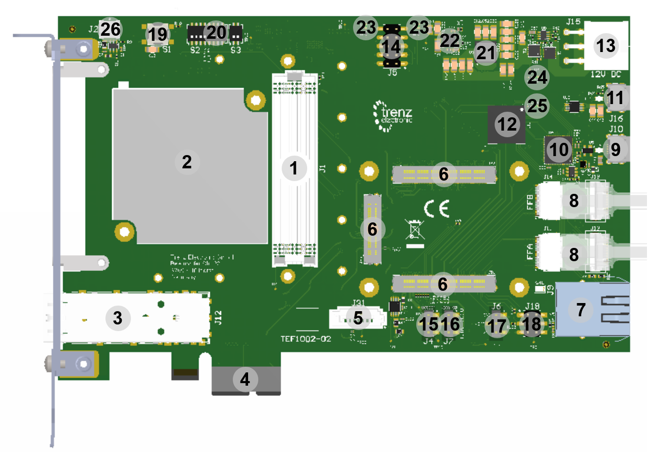
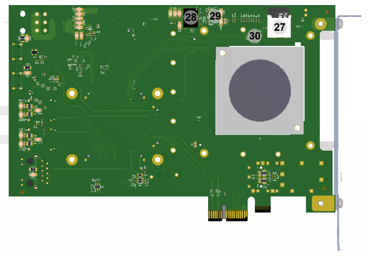
- ANSI/VITA 57.1 compliant FMC LPC connector, J1
- Cooling fan 5VDC M1 (45X5MM, 0.7W, 1.06CFM), M1
- SFP+ connector, J12
- PCIe x1 connector, J3
- SATA connector with pin 7 power configuration, J31
- Trenz Electronic 4 x 5 modules B2B connectors, JB1 ... JB3
- RJ45 Gigabit Ethernet connector, J9
- 2x high speed LVDS arrangement of connectors J11, J13, J14, J18
- Micro-USB2 connector, J10
- FTDI FT2232H USB2 to JTAG,UART/FIFO Bridge, U4
- Micro-USB2 connector, J16
- MAX10 10M08SAU169C8G CPLD, U11
- 6-pin 12V power connector, J15
- 6x1 5x2 JTAG pin header (not fitted)for TEI0004, J5
- 3x1 jumper pin header (select VCCIOA), J4
- 3x1 jumper pin header (select VCCA_SD), J7
- 2x1 3x1 pin header (VBAT), J6
- 2x5 1,27mm pitch 2x3 pin header (MIO/PJTAG), J19
- Push button, S1
- 10x dip switch, S2, S3
- DCDC LMZ23605TZ @5.0V (5V0PER), U15DCDC LMZ23605TZ LTM4638 @5.0V (5V0), U9
- DCDC LMZ23605TZ EN6338QI @3.3V(3V3IN), U10
- 2x green LED (user), D1, D2
- green LED (Power), D3
- green LED (Status), D4
- SD-Card connector (top loader),
- DCDC EN5335QI (FMC_VADJ), U1
- DCDC EN6338QI @3.3V (3V3FMC), U14
- SDIO Level shifter TXS02612, U3
...
| Scroll Title |
|---|
| anchor | Table_OV_CS |
|---|
| title | TEF1002 Control Signals |
|---|
|
| Scroll Table Layout |
|---|
| orientation | portrait |
|---|
| sortDirection | ASC |
|---|
| repeatTableHeaders | default |
|---|
| sortByColumn | 1 |
|---|
| sortEnabled | false |
|---|
| cellHighlighting | true |
|---|
|
Control signal | Switch / Button / LED / Pin | Signal Schematic Names | Connected to | Functionality | Notes |
|---|
| FMC_VADJ voltage selection | DIP switches S2-1, S2-2, S2-3 | VID0 ... VID2 | SC CPLD U11, pins K6, J5, K5 | sets adjustable voltage for FMC connector | dependens on SC CPLD configuration | | JTAG enable | DIP switch S2-4 | JTAGEN | SC CPLD U11, pin E5 | OFF: TEF1002 SC CPLD Module/FMC JTAG enabled,
ON: Module/FMC TEF1002 SC CPLD JTAG enabled, | - | | Module JTAG select | DIP switch S2-5 | M_JTAGEN | B2B JB1, pin 90 | When S2-4 ON and S2-6 OFF: OFF: Module SC CPLD SOC JTAG enabled, ON: Module SOC SC CPLD JTAG enabled | - | | FMC JTAG select | DIP switch S2-6 | FMC_JTAG | SC CPLD U11,L3 | When S2-4 ON: OFF: TEF1002 SC CPLD JTAG enabled, ON: FMC JTAG enabled | depends on SC CPLD configuration, only avialiable when 4x5 module installed | | Enable module power | DIP switch S2-7 | CM0 | SC CPLD U11, M3 | Module power. Set ON to enable module power. (Power management depends on module. ) | depends on SC CPLD configuration, only avialiable when 4x5 module installed | | No sequenzing | DIP switch S2-8 | CM1 | SC CPLD U11, L2 | Module Power management. Set ON to disable module CPLD power management. Power management depends on module and not all modules support extended power management with CPLD. | depends on SC CPLD configuration, only avialiable when 4x5 module installed | | Boot Mode | DIP switch S3-1 | CM2 | SC CPLD U11, K2 | Boot Mode for attached module (Default: OFF for primary SD boot and ON for primary QSPI boot. Depends also on module CPLD firmware). | depends on SC CPLD configuration, only avialiable when 4x5 module installed | | FMC VADJ enable | DIP switch S3-2 | USR0 | SC CPLD U11, K1 | ON: FMC VADJ enable also without installed FMC Card OFF: FMC_FADJ only enabled when FMC installed. | dependens on SC CPLD configuration, only avialiable when 4x5 module installed | | Reset | Push button S1 | BUTTON | SC CPLD U11, N6 | Module Reset, Low active module reset. Pin force Power one reset on FPGA/SoC. | depends on SC CPLD configuration | | 2x User LED | Green LEDs D1, D2 | LED1, LED2 | SC CPLD U11, J5, K5 | Depends on User configuration, curenntly both off, if not otherwise programmed. | depends on SC CPLD configuration | | Board power indicator | Green LED D3 | 3V3IN | B2B JB1, pin 14, 16 | ON: 3.3V on-board voltage available | - | | Board status indicators | Green LED D4 | - | SC CPLD U11, pin C2 | ON: No failure. For other blinking status of this LED please refer to SC Firmware description. | dependens on SC CPLD configuration | | Enable module power | SC CPLD U11, D11 | EN1 | B2B JB1, pin 27 | Module power. (Power management depends on module. ) | - | | No sequenzing | SC CPLD U11, E13 | NOSEQ | B2B JB1, pin 8 | Power management depends on module and not all modules support extended power management with CPLD. | - | | Boot Mode | SC CPLD U11, B11 | MODE | B2B JB1, pin 31 | Boot Mode for attached module. LOW for primary SD boot and HIGH for primary QSPI boot. (Depends also on module CPLD firmware). | - | | Module Reset | SC CPLD U11, E12 | RESIN | B2B JB2, pin 17 | Module Reset | - |
|
...
| Scroll Title |
|---|
| anchor | Table_SIP_SDC |
|---|
| title | micro SD-Card connector |
|---|
|
| Scroll Table Layout |
|---|
| orientation | portrait |
|---|
| sortDirection | ASC |
|---|
| repeatTableHeaders | default |
|---|
| sortByColumn | 1 |
|---|
| sortEnabled | false |
|---|
| cellHighlighting | true |
|---|
|
| Connector J8 pin | Signal Schematic Name
| Muxed to signal on Port Expander | Connected to | Notes |
|---|
| 2, DAT3 | SD-D3_LS | SD_D3 | B2B JB1, pin 18 | - | 3, CMD | SD-CMD_LS | SD_CMD | B2B JB1, pin 26 | - | 5, CLK | SD-CCLK_LS | SD_CCLK | B2B JB1, pin 28 | - | 7, DAT0 | SD-D0_LS | SD_D0 | B2B JB1, pin 24 | - | 8, DAT1 | SD-D1_LS | SD_D1 | B2B JB1, pin 22 | - | 1, DAT2 | SD-D2_LS | SD_D2 | B2B JB1, pin 20 | - | | 9, CARD Detect | SD-CD | - | U11, pin M1 | CPLD Firmware dependent, in default firmware not used |
|
On-board Peripherals
| Page properties |
|---|
|
Notes : - add subsection for every component which is important for design, for example:
- Ethernet PHY
- USB PHY
- Programmable Clock Generator
- Oscillators
- eMMCs
- RTC
- FTDI
- ...
- DIP-Switches
- Buttons
- LEDs
|
...
| Scroll Title |
|---|
| anchor | Table_RH_HRH |
|---|
| title | Hardware Revision History |
|---|
|
| Scroll Table Layout |
|---|
| orientation | portrait |
|---|
| sortDirection | ASC |
|---|
| repeatTableHeaders | default |
|---|
| sortByColumn | 1 |
|---|
| sortEnabled | false |
|---|
| cellHighlighting | true |
|---|
|
| Date | Revision | Note | PCN | Documentation Link |
|---|
| 2020-01-29 | 02 | Prototypes | - | - | | - | 01 | Prototypes | - | - |
|
| Scroll Title |
|---|
| anchor | Figure_RH_HRN |
|---|
| title | Hardware Revision Number |
|---|
|
| draw.io Diagram |
|---|
| border | true |
|---|
| viewerToolbar | true |
|---|
| fitWindow | false |
|---|
| diagramName | HRN_TEF1002 |
|---|
| simpleViewer | false |
|---|
| diagramWidth | 406 |
|---|
| revision | 1 |
|---|
|
|
...
| Scroll Title |
|---|
| anchor | Table_RH_DCH |
|---|
| title | Document change history. |
|---|
|
| Scroll Table Layout |
|---|
| orientation | portrait |
|---|
| sortDirection | ASC |
|---|
| repeatTableHeaders | default |
|---|
| sortByColumn | 1 |
|---|
| sortEnabled | false |
|---|
| cellHighlighting | true |
|---|
|
| Date | Revision | Contributor | Description |
|---|
| Page info |
|---|
| infoType | Modified date |
|---|
| dateFormat | yyyy-MM-dd |
|---|
| type | Flat |
|---|
|
| | Page info |
|---|
| infoType | Current version |
|---|
| prefix | v. |
|---|
| type | Flat |
|---|
| showVersions | false |
|---|
|
| | Page info |
|---|
| infoType | Modified by |
|---|
| type | Flat |
|---|
| showVersions | false |
|---|
|
| | | 2019-09-06 | v.25 | Martin Rohrmüller | | -- | all | | Page info |
|---|
| infoType | Modified users |
|---|
| type | Flat |
|---|
| showVersions | false |
|---|
|
| |
|
...