| Scroll Table Layout |
|---|
| orientation | portrait |
|---|
| sortDirection | ASC |
|---|
| repeatTableHeaders | default |
|---|
| style | |
|---|
| widths | |
|---|
| sortByColumn | 1 |
|---|
| sortEnabled | false |
|---|
| cellHighlighting | true |
|---|
|
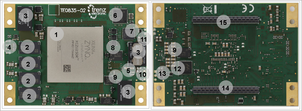
| FPGA Bank | B2B Connector | Number of I/Os | Voltage Level | Notes |
|---|
| Bank 500 | J1 | 12x Single Ended | 1.8V | MIO14...25 | | Bank 501 | J1 | 20x Single Ended | 1.8V | MIO26...51 | | Bank 505 | J1 | 18x Single Ended, 9x Differential pairs | 0.85V | EXT_CLKIN_PSMGT, RX/TX0...3 | | Bank 128 | J1 | 18x Single Ended, 9x Differential pairs | 0.9V | B128_CLK, RX/TX0...3 | | Bank 129 | J1 | 18x Single Ended, 9x Differential pairs | 0.9V | B129_CLK, RX/TX0...3 | | Bank 65 | J2 | 24x Single Ended, 12x Differential pairs | 1.8V |
| | Bank 88 | J2 | 16x Single Ended, 8x Differential pairs | 3.3V | HD_B88 |
|