...
The Trenz Electronic TE0835 is an extended-grade module based on Xilinx Zynq UltraScale+ RFSoC. The module is equipped with 4x 8Gb DDR4 SDRAM Memory, 2x 512Mb SPI Flash Memory, USB2.0, Ethernet Transceiver and 2x Samtec Razor Beam Borard to Board (B2B) Connectors. The system controller CPLD is provided by Lattice MachXO2.
The Zynq UltraScale+ RFSoC family integrates key subsystems for multiband, multi-mode cellular radios and cable infrastructure (DOCSIS) into an SoC platform that contains a feature-rich 64-bitquad-core Arm Cortex-A53 and dual-core Arm Cortex-R5 based processing system.
Refer to http://trenz.org/te0835-info for the current online version of this manual and other available documentation.
...
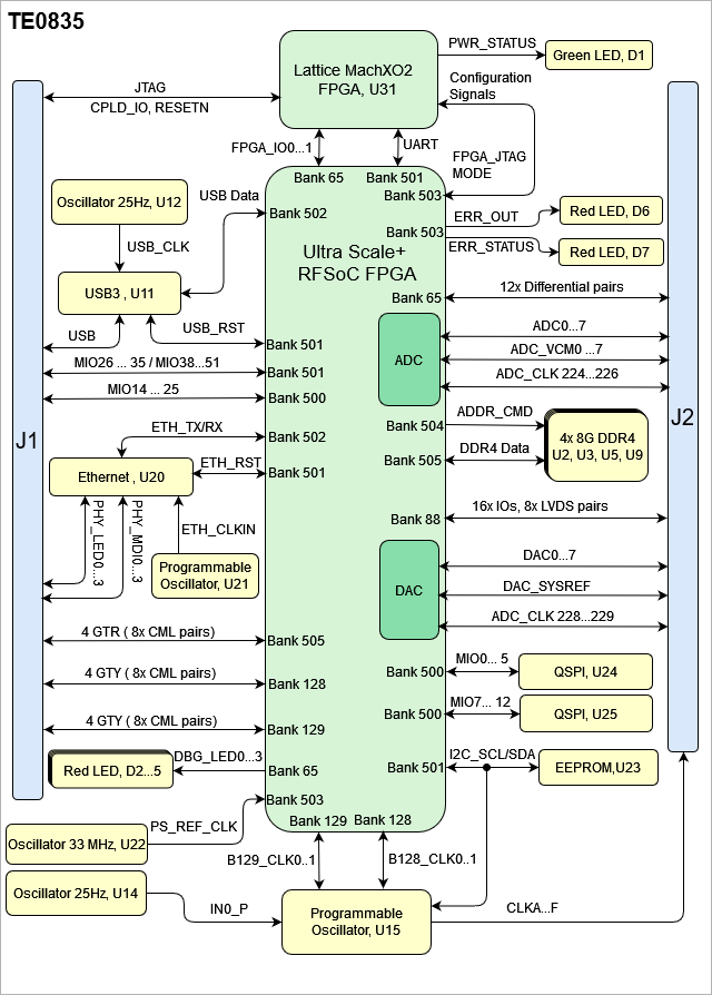
| Scroll Title |
|---|
| anchor | Figure_OV_BD |
|---|
| title | TE0835 block diagram |
|---|
|
| Scroll Ignore |
|---|
| draw.io Diagram |
|---|
| border | false |
|---|
| viewerToolbar | true |
|---|
| |
|---|
| fitWindow | false |
|---|
| diagramDisplayName | |
|---|
| lbox | true |
|---|
| revision | 34 |
|---|
| diagramName | TE0835_OV_BD |
|---|
| simpleViewer | false |
|---|
| width | |
|---|
| links | auto |
|---|
| tbstyle | hidden |
|---|
| diagramWidth | 641 |
|---|
|
|
| Scroll Only |
|---|
|
|
...
| Scroll Title |
|---|
| anchor | Table_SIP_TPs |
|---|
| title | Test Points Information |
|---|
|
| Scroll Table Layout |
|---|
| orientation | portrait |
|---|
| sortDirection | ASC |
|---|
| repeatTableHeaders | default |
|---|
| style | |
|---|
| widths | |
|---|
| sortByColumn | 1 |
|---|
| sortEnabled | false |
|---|
| cellHighlighting | true |
|---|
|
| Test Point | Signal | Connected to | Notes |
|---|
| TP1 | CLKOUT | Voltage Regulator, U7 |
| | TP2 | PLL_RSTN | Programmable Clock Generator, U15 |
| | TP3 | 3.3V_CPLD | B2B, J1 |
| | TP4 | CPLD_JTAGEN | B2B, J1 CPLD, U31 |
| | TP5 | JTAG_TDO | B2B, J1 CPLD, U31 |
| | TP6 | JTAG_TDI | B2B, J1 CPLD, U31 |
| | TP7 | JTAG_TCK | B2B, J1 CPLD, U31 |
| | TP8 | JTAG_TMS | B2B, J1 CPLD, U31 |
| | TP9 | GND | GND |
| | TP10...11 | IO_L1P_AD15P_88, O_L4N_AD12N_88 | FPGA Bank 88, U1 |
| | TP12 | VIN | B2B, J1 |
| | TP13...14 | GND | GND |
| | TP15...16 | MIO32-MIO33 | EEPROM,U23 FPGA Bank 501, U1 |
| | TP17 | GND | GND |
| | TP18 | ADC_AVCC | LDO Voltage Regulator, U8 |
| | TP19 | ADC_AVCCAUX | LDO Voltage Regulator, U10 |
|
|
On-board Peripherals
| Page properties |
|---|
|
Notes : - add subsection for every component which is important for design, for example:
- Two 100 Mbit Ethernet Transciever PHY
- USB PHY
- Programmable Clock Generator
- Oscillators
- eMMCs
- RTC
- FTDI
- ...
- DIP-Switches
- Buttons
- LEDs
|
...
| Scroll Title |
|---|
| anchor | Table_OBP |
|---|
| title | On board peripherals |
|---|
|
| Scroll Table Layout |
|---|
| orientation | portrait |
|---|
| sortDirection | ASC |
|---|
| repeatTableHeaders | default |
|---|
| style | |
|---|
| widths | |
|---|
| sortByColumn | 1 |
|---|
| sortEnabled | false |
|---|
| cellHighlighting | true |
|---|
|
|
Quad SPI Flash Memory
| Page properties |
|---|
|
Notes : Minimum and Maximum density of quad SPI flash must be mentioned for other assembly options. |
...
| Scroll Title |
|---|
| anchor | Table_OBP_SPI |
|---|
| title | Quad SPI interface MIOs and pins |
|---|
|
| Scroll Table Layout |
|---|
| orientation | portrait |
|---|
| sortDirection | ASC |
|---|
| repeatTableHeaders | default |
|---|
| style | |
|---|
| widths | |
|---|
| sortByColumn | 1 |
|---|
| sortEnabled | false |
|---|
| cellHighlighting | true |
|---|
|
| MIO Pin | Schematic | U24 Pin | U25 Pin | Notes |
|---|
| MIO0 | MIO0_QSPI | CLK | - |
| | MIO1 | MIO1_QSPI | DO | - |
| | MIO2 | MIO2_QSPI | nWP | - |
| | MIO3 | MIO3_QSPI | nHOLD | - |
| | MIO4 | MIO4_QSPI | DI | - |
| | MIO5 | MIO5_QSPI | nCS | - |
| | MIO7 | MIO5_QSPI | - | nCS |
| | MIO8 | MIO5_QSPI | - | DI |
| | MIO9 | MIO5_QSPI | - | DO |
| | MIO10 | MIO5_QSPI | - | nWP |
| | MIO11 | MIO5_QSPI | - | nHOLD |
| | MIO12 | MIO5_QSPI | - | CLK |
|
|
System Controller CPLD
The System Controller CPLD (U31) is provided by Lattice Semiconductor LCMXO2-460HC. The SC-CPLD is the central system management unit where essential control signals are logically linked by the implemented logic in CPLD firmware, which generates output signals to control the system, the on-board peripherals and the interfaces. Interfaces like JTAG / UART and I2C between the on-board peripherals and the attached module are by-passed, forwarded and controlled by the System Controller CPLD.
...
| Scroll Title |
|---|
| anchor | Table_OBP_USB |
|---|
| title | USB2.0 interface connections and pins |
|---|
|
| Scroll Table Layout |
|---|
| orientation | portrait |
|---|
| sortDirection | ASC |
|---|
| repeatTableHeaders | default |
|---|
| style | |
|---|
| widths | |
|---|
| sortByColumn | 1 |
|---|
| sortEnabled | false |
|---|
| cellHighlighting | true |
|---|
|
| Schematic/Pin | Connected to | Description | Note |
|---|
| MODE0...3 | FPGA Bank 503, U1 | Boot Mode |
| | POR_B | FPGA Bank 503, U1 | Programming Status | Pulled up | | PORG_B | FPGA Bank 503, U1 | Programming Status | Pulled up | | INIT_B | FPGA Bank 503, U1 | Configuration initialization | Pulled up | | DONE | FPGA Bank 503, U1 | Configuration Done Status | Pulled up | | F_TCK | FPGA Bank 503, U1 | FPGA JTAG |
| | F_TDI | FPGA Bank 503, U1 | FPGA JTAG |
| | F_TMS | FPGA Bank 503, U1 | FPGA JTAG |
| | F_TDO | FPGA Bank 503, U1 | FPGA JTAG |
| | JTAG_TDO | B2B, J1 | CPLD JTAG |
| | JTAG_TMS | B2B, J1 | CPLD JTAG |
| | JTAG_TDI | B2B, J1 | CPLD JTAG |
| | JTAG_TCK | B2B, J1 | CPLD JTAG |
| | CPLD_JTAGEN | B2B, J1 | CPLD JTAG Enable |
| | CPLDIO0...3 | B2B, J1 | CPLD IOs |
| | RESETN | B2B, J1 | Reset |
| | MIO13 | LED Green, D1 | 3.3V_CPLD |
| | MIO28 | FPGA Bank 501, U1 | UART_TX |
| | MIO29 | FPGA Bank 501, U1 | UART_RX |
| | FPGA_IO0...1 | FPGA Bank 65, U1 | IOs |
| | EN_PS_PL | Voltage Regulators, U6, U7, U29 | PS/PL Enable Signals | Pulled Down | | EN_GR1 | Voltage Regulators, U19, U27, U28 | MGTAVTT, PSLL | Pulled Down | | EN_GR2 | Voltage Regulators, U38, U18, U38 | PS_MGTRAVTT, 3.3, DDR2.5V | Pulled Down | | EN_RF_ADC | Voltage Regulators, U8 | Enable ADC | Pulled Down | | PG_RF_DAC | Voltage Regulators, U17 | ADC Power Good Status | Pulled Down | | PG_PS_PL | Voltage Regulators, U6, U7, U29 | PS/PL Power Good Status | Pulled Down | | EN_RF_DAC | Voltage Regulators, U13 | Enable DAC | Pulled Down | | PG_RF_DAC | Voltage Regulators, U10 | DAC Power Good Status | Pulled Down |
|
USB2.0
The TE0835 is equipped with a USB2.0, U11.
| Scroll Title |
|---|
| anchor | Table_OBP_USB |
|---|
| title | USB2.0 interface connections and pins |
|---|
|
| Scroll Table Layout |
|---|
| orientation | portrait |
|---|
| sortDirection | ASC |
|---|
| repeatTableHeaders | default |
|---|
| style | |
|---|
| widths | |
|---|
| sortByColumn | 1 |
|---|
| sortEnabled | false |
|---|
| cellHighlighting | true |
|---|
|
| U11 Pin | Schematic | Connected to | Notes |
|---|
| RESETB | USB0_RST | FPGA Bank 501, U1 |
| | VDDIO | 1.8V | 1.8V |
| | CPEN | USB0_CPE | B2B, J1 |
| | VBUS | USB0_VBUS | B2B, J1 |
| | ID | USB0_ID | B2B, J1 |
| | DP | USB0_D_P | B2B, J1 |
| | DM | USB0_D_N | B2B, J1 |
| | REFCLK | USB_CLK | Oschillator, U12 |
| | STP | USB0_STP | FPGA Bank 502, U1 |
| | NXT | USB0_NXT | FPGA Bank 502, U1 |
| | DIR | USB0_DIR | FPGA Bank 502, U1 |
| | CLKOUT | USB_CLK | Oschillator, U12 |
| | DATA0...7 | USB0_DATA0...8 | FPGA Bank 502, U1 |
|
|
Ethernet
The module TE0835 is equipped with a Gigabit Ethernet Transceiver, U20.
| Scroll Title |
|---|
| anchor | Table_OBP_ETH |
|---|
| title | Ethernet connections |
|---|
|
| Scroll Table Layout |
|---|
| orientation | portrait |
|---|
| sortDirection | ASC |
|---|
| repeatTableHeaders | default |
|---|
| style | |
|---|
| widths | |
|---|
| sortByColumn | 1 |
|---|
| sortEnabled | false |
|---|
| cellHighlighting | true |
|---|
|
| U20 Pin | Signal Name | Connected to | Signal Description | Note |
|---|
| MDIO | ETH_MDIO | FPGA Bank 502, U1 | Data Management |
| | MDC | ETH_MDC | FPGA Bank 502, U1 | Data Management clock reference for the serial interface |
| | TX_CLK | ETH_TXCK | FPGA Bank 502, U1 | Transmit Clock |
| | TX_CTRL | ETH_TXCTL | FPGA Bank 502, U1 | Transmit Control |
| | TXD0...3 | ETH_TXD0...3 | FPGA Bank 502, U1 | Transmit Data |
| | RX_CLK | ETH_RXCK | FPGA Bank 502, U1 | Receive Clock |
| | RX_CTRL | ETH_RXCTL | FPGA Bank 502, U1 | Receive Control |
| | RXD0...3 | ETH_RXD0...3 | FPGA Bank 502, U1 | Receive Data |
| | RESETn | ETH_RST | FPGA Bank 501, U1 | Ethernet reset, Active low. |
| | XTAL_IN | ETH_XTAL_IN | Oscillator, U21 | Reference Clock |
| MDI0...3 | PHY_MDI0...3 | B2B, J1 | Media Dependent Interface 0...3 |
| | LED0...1 | PHY_LED0...1 | B2B, J1 | LED output |
| | LED/INT | PHY_LED2 | B2B, J1 | LED interrupt |
|
|
EEPROM
The module TE0835 has an EEPROM (U23) connected to PSMIO FPGA Bank 501.
...
| Scroll Title |
|---|
| anchor | Figure_PWR_PD |
|---|
| title | Power Distribution |
|---|
|
| Scroll Ignore |
|---|
| draw.io Diagram |
|---|
| border | false |
|---|
| viewerToolbar | true |
|---|
| |
|---|
| fitWindow | false |
|---|
| diagramDisplayName | |
|---|
| lbox | true |
|---|
| revision | 810 |
|---|
| diagramName | TE0835_PWR_PD |
|---|
| simpleViewer | false |
|---|
| width | |
|---|
| links | auto |
|---|
| tbstyle | hidden |
|---|
| diagramWidth | 641 |
|---|
|
|
| Scroll Only |
|---|

|
|
...
| Scroll Title |
|---|
| anchor | Table_PWR_PR |
|---|
| title | Module power rails. |
|---|
|
| Scroll Table Layout |
|---|
| orientation | portrait |
|---|
| sortDirection | ASC |
|---|
| repeatTableHeaders | default |
|---|
| style | |
|---|
| widths | |
|---|
| sortByColumn | 1 |
|---|
| sortEnabled | false |
|---|
| cellHighlighting | true |
|---|
|
JM1 B2B Connector B2B Connector JM2 B2B J2 Pin | Direction | Notes |
|---|
| VIN | 1,2,3,4,5,6,8 | - | Input |
| | PSBATT | 14 | - | Input |
| | 3.3V_CPLD | 16 | - | Output |
|
|
Bank Voltages
| Scroll Title |
|---|
| anchor | Table_PWR_BV |
|---|
| title | Zynq SoC bank voltages. |
|---|
|
| Scroll Table Layout |
|---|
| orientation | portrait |
|---|
| sortDirection | ASC |
|---|
| repeatTableHeaders | default |
|---|
| style | |
|---|
| widths | |
|---|
| sortByColumn | 1 |
|---|
| sortEnabled | false |
|---|
| cellHighlighting | true |
|---|
|
| Schematic Name | | Notes |
|---|
| Bank 65 HP | VCCO_65 | 1.8V |
| | Bank 503 PSCONFIG | VCCO_PSIO3_503 | 1.8V |
| | Bank 88 HD | VCCO_88 | 3.3V |
| | BANK 128 GTH | MGTAVCC | 0.9V |
| | BANK 129 GTH | MGTAVCC | 0.9V |
| | BANK 500 PSMIO | VCCO_PSIO0_500 | 1.8V |
| | BANK 501 PSMIO | VCCO_PSIO0_501 | 1.8V |
| | BANK 502 | VCCO_PSIO0_502 | 1.8V |
| | BANK 504 PSDDR | VCCO_PSDDR_504 | 1.2V |
| | BANK 505 PSGTR | PS_MGTRAVCC | 0.85V |
|
|
Board to Board Connectors
...
| Scroll Title |
|---|
| anchor | Table_TS_AMR |
|---|
| title | PS absolute maximum ratings |
|---|
|
| Scroll Table Layout |
|---|
| orientation | portrait |
|---|
| sortDirection | ASC |
|---|
| repeatTableHeaders | default |
|---|
| style | |
|---|
| widths | |
|---|
| sortByColumn | 1 |
|---|
| sortEnabled | false |
|---|
| cellHighlighting | true |
|---|
|
| Symbols | Description | Min | Max | Unit |
|---|
| VIN | Input Supply Voltage | 0 | 5 | V | | T_STG | Storage Temperature | -40 | 100 | °C |
|
Recommended Operating Conditions
...