...
Key Features
| Page properties |
|---|
|
Note:
'description: Important components and connector or other Features of the module
→ please sort and indicate assembly options Key Features' must be split into 6 main groups for modules and mainboards: - SoC/FPGA
- Package: SFVC784
- Device: ZU2...ZU5*
- Engine: CG, EG, EV*
- Speed: -1LI, -2LE,*, **
- Temperature: I, E,*, **
- RAM/Storage
- Low Power DDR4 on PS
- Data width: 32bit
- Size: def. 2GB*
- Speed:***
- eMMC
- Data width: 8Bit
- size: def. 8GB *
- QSPI boot Flash in dual parallel mode (size depends on assembly version)
- Data width: 8bit
- size: def. 128MB *
- HyperRAM/Flash (optional, default not assembled)
- MAC address serial EEPROM with EUI-48™ node identity (Microchip 24AA025E48)
- On Board
- Lattice LCMXO2
- PLL SI5338
- Gigabit Ethernet transceiver PHY (Marvell Alaska 88E1512)
- Hi-speed USB2 ULPI transceiver with full OTG support (Microchip USB3320C)
- Interface
- 132 x HP PL I/Os (3 banks)
- ETH
- USB
- 4 GTR (for USB3, Sata, PCIe, DP)
- MIO for UART
- MIO for SD
- MIO for PJTAG
- JTAG
- Ctrl
- Power
- 3.3V-5V Main Input
- 3.3V Controller Input
- Variable Bank IO Power Input
- Dimension
- Notes
- * depends on assembly version
- ** also non low power assembly options possible
- *** depends on used U+ Zynq and DDR4 combination
Key Features' must be split into 6 main groups for carrier: - Modules
- TE0808, TE807, TE0803,...
- RAM/Storage
- On Board
- Interface
- E.g. ETH, USB, B2B, Display port
- Power
- E.g. Input supply voltage
- Dimension
|
Intel® MAX 10 Commercial [10M08SAU169C8G]
SDRAM Memory up to 64Mb, 166MHz
Dual High Speed USB to Multipurpose UART/FIFO IC
64 Mb Quad SPI Flash - No on all variants
4Kb EEPROM Memory
8x User LED
Micro USB2 Receptacle 90
18 Bit 2 MSPS Analog to Digital Converter
2x SMA Female Connector
I/O interface: 23x GPIO
Power Supply: 5V
Dimension: 86.5mm x 25mm
- Fully-Differential Programmable-Gain Instrumentation Amplifier
...
| Scroll Title |
|---|
| anchor | Table_OBP_IOs |
|---|
| title | FPGA I/O Banks |
|---|
|
| Scroll Table Layout |
|---|
| orientation | portrait |
|---|
| sortDirection | ASC |
|---|
| repeatTableHeaders | default |
|---|
| style | |
|---|
| widths | |
|---|
| sortByColumn | 1 |
|---|
| sortEnabled | false |
|---|
| cellHighlighting | true |
|---|
|
| FPGA Bank | I/O Signal Count | Connected to | Notes |
|---|
| Bank 1A | 7 | 1x14 Pin header, J1 | AIN0...6 | | 1 | Jumper, J3 | AIN7 | | Bank 1B | 5 | 1x6 Pin header, J4 | JTAG_EN, TDI, TDO, TMS, TCK | Bank 2
| 1 | 12MHz Oscillator, U7 | CLK12M | | 4 | 1x14 Pin header, J1 | D2...5 | | 4 | A2D, U6 | ADC_SDI, ADC_SDO, ADC_SCK, ADC_CNV | | 3 | Amplifier, U12 | AMP_A0, AMP_A1, AMP_A2 | | 1 | A2D, U6 | ADC_PWR_EN1 | | 1 | 100MHz Oscillator, U19 | CLK_EN | | Bank 3 | 22 | SDRAM, U2 | RAM_ADDR_CMD | | 1 | A2D, U6 | PDB_AMP | | Bank 5 | 9 | 1x14 Pin header, J2 | DIO6...14 | | 2 | 1x14 Pin header, J1 | DIO0...1 | | 1 | D12_R | DIO12 | | Bank 6 | 16 | SDRAM, U2 | DQ0...15 | | 2 | SDRAM, U2 | DQM0...1 | | 1 | D11_R | DIO11 | | 1 | A2D, U6 | PDB_REF | Bank 8
| 8 | User Red LEDs, D2...9 | LED1...8 | | 6 | SPI Flash, U5 | F_CS, F_CKL, F_DI, F_DO, nSTATUS, DEVCLRn | | 1 | Red LED, D10 | CONF_DONE | | 6 | FTDI JTAG/UART Adapter, U3 | BDBUS0...5 | | 1 | Push Button, S2 | USER_BTN |
|
Micro-USB2 Connector
The Micro-USB2 connector J9 provides an interface to access the UART and JTAG functions via FTDI FT2232 chip. The use of this feature requires that USB driver is installed on your host PC.
...
The TEI0023 board is equipped with the Analog Devices ADAQ4003BBCZ 18-bit 2MSPS ADC.
| Scroll Title |
|---|
| anchor | Table_OBP_A2D |
|---|
| title | A2D converter interface and pins |
|---|
|
| Scroll Table Layout |
|---|
| orientation | portrait |
|---|
| sortDirection | ASC |
|---|
| repeatTableHeaders | default |
|---|
| style | |
|---|
| widths | |
|---|
| sortByColumn | 1 |
|---|
| sortEnabled | false |
|---|
| cellHighlighting | true |
|---|
|
| Pins | Connected to | Notes |
|---|
IN+ | Instrumentation Amplifier U14, VOUT- |
| | IN- | Instrumentation Amplifier U14, VOUT+ |
| | SDI | FPGA, Bank 2, pin M2, ADC_SDI |
| | SDO | FPGA, Bank 2, pin M1, ADC_SDO |
| | SCK | FPGA, Bank 2, pin N3, ADC_SCK |
| | CNV | FPGA, Bank 2, pin N2, ADC_CNV |
|
|
...
| Scroll Title |
|---|
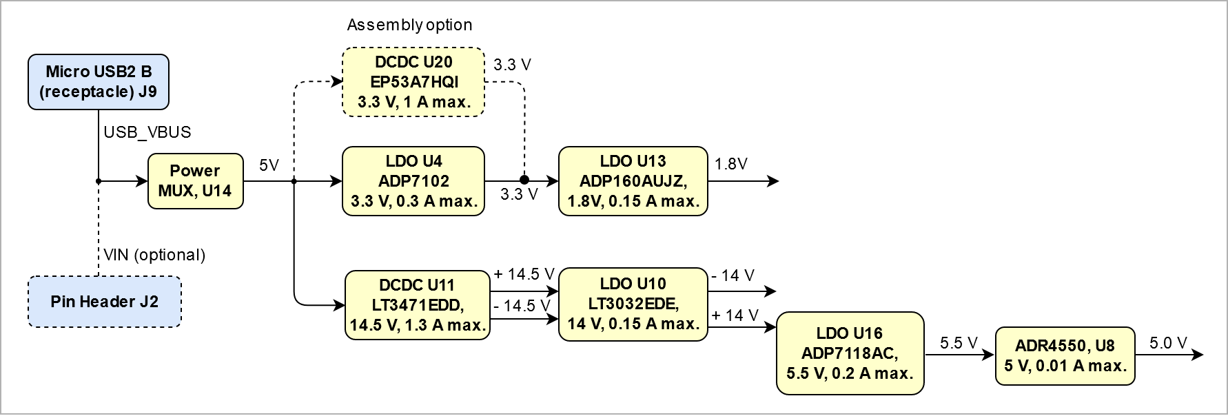
| anchor | Figure_PWR_PD |
|---|
| title | Power Distribution |
|---|
|
| Scroll Ignore |
|---|
| draw.io Diagram |
|---|
| border | true |
|---|
| viewerToolbar | true |
|---|
| |
|---|
| fitWindow | false |
|---|
| diagramName | TEI0023_PWR_PD |
|---|
| simpleViewer | false |
|---|
| width | |
|---|
| diagramWidth | 891 |
|---|
| revision | 2 |
|---|
|
|
| Scroll Only |
|---|
|
|
Power-On Sequence
There is no specific or special power-on sequence, just one single power source is needed. After power on the green LED (D1) will be on.
Power Rails
| Scroll Title |
|---|
| anchor | Table_PWR_PR |
|---|
| title | Module power rails. |
|---|
|
| Scroll Table Layout |
|---|
| orientation | portrait |
|---|
| sortDirection | ASC |
|---|
| repeatTableHeaders | default |
|---|
| style | |
|---|
| widths | |
|---|
| sortByColumn | 1 |
|---|
| sortEnabled | false |
|---|
| cellHighlighting | true |
|---|
|
| Power Rail Name | Connector J2 Pin | Connector J9 Pin | Direction | Notes |
|---|
| VIN | J2-13 | - | Input | 5 V - Pin Header | | 3.3V | J2-12 | - | Output |
| | 5V | J2-14 | - | Output |
| USB_VBUS | - | J9-1 | Input | 5 V - USB Connector |
|
...
| Scroll Title |
|---|
| anchor | Table_RH_DCH |
|---|
| title | Document change history. |
|---|
|
| Scroll Table Layout |
|---|
| orientation | portrait |
|---|
| sortDirection | ASC |
|---|
| repeatTableHeaders | default |
|---|
| style | |
|---|
| widths | |
|---|
| sortByColumn | 1 |
|---|
| sortEnabled | false |
|---|
| cellHighlighting | true |
|---|
|
| Date | Revision | Contributor | Description |
|---|
| Page info |
|---|
| infoType | Modified date |
|---|
| dateFormat | yyyy-MM-dd |
|---|
| type | Flat |
|---|
|
| | Page info |
|---|
| infoType | Current version |
|---|
| prefix | v. |
|---|
| type | Flat |
|---|
| showVersions | false |
|---|
|
| | Page info |
|---|
| infoType | Modified by |
|---|
| type | Flat |
|---|
| showVersions | false |
|---|
|
| | -- | all | | Page info |
|---|
| infoType | Modified users |
|---|
| type | Flat |
|---|
| showVersions | false |
|---|
|
| |
|
Disclaimer
| Include Page |
|---|
| IN:Legal Notices |
|---|
| IN:Legal Notices |
|---|
|