...
The Trenz Electronic TE0823 (3PIU1FA /3PIU1FL) is an industrial-grade MPSoC module integrating a low power Xilinx Zynq UltraScale+ ZU3CGMPSoC, 1 GByte LPDDR4 SDRAM, 128 MByte , 8 GB eMMC chip, 2x 64 MB Flash memory for configuration and operation, and powerful switch-mode power supplies for all on-board voltages. A large number of configurable I/O's is provided via rugged high-speed stacking connections.. The module is equipped with a Lattice Mach XO2 CPLD for system controlling. 3x Robust high-speed connectors provide a large number of inputs and outputs.
The highly integrated modules are All this on a tiny footprint, smaller than a credit card , at the most competitive price. Modules in and are offered in several variants at an affordable price-performance ratio. Modules with a 4 x 5 cm form factor are fully completely mechanically and largely electrically compatible among with each other.
All parts are at least industrial temperature range of -40°C to +85°C. The module operating temperature range depends on customer design and cooling solution. Please contact us for options.
Refer to http://trenz.org/te0823-info for the current online version of this manual and other available documentation.
...
| Page properties |
|---|
|
Note:
'description: Important components and connector or other Features of the module
→ please sort and indicate assembly options Key Features' must be split into 6 main groups for modules and mainboards: - SoC/FPGA
- Package: SFVC784
- Device: ZU2...ZU5*
- Engine: CG, EG, EV*
- Speed: -1LI, -2LE,*, **
- Temperature: I, E,*, **
- RAM/Storage
- Low Power DDR4 on PS
- Data width: 32bit
- Size: def. 2GB*
- Speed:***
- eMMC
- Data width: 8Bit
- size: def. 8GB *
- QSPI boot Flash in dual parallel mode (size depends on assembly version)
- Data width: 8bit
- size: def. 128MB *
- HyperRAM/Flash (optional, default not assembled)
- MAC address serial EEPROM with EUI-48™ node identity (Microchip 24AA025E48)
- On Board
- Lattice LCMXO2
- PLL SI5338
- Gigabit Ethernet transceiver PHY (Marvell Alaska 88E1512)
- Hi-speed USB2 ULPI transceiver with full OTG support (Microchip USB3320C)
- Interface
- 132 x HP PL I/Os (3 banks)
- ETH
- USB
- 4 GTR (for USB3, Sata, PCIe, DP)
- MIO for UART
- MIO for SD
- MIO for PJTAG
- JTAG
- Ctrl
- Power
- 3.3V-5V Main Input
- 3.3V Controller Input
- Variable Bank IO Power Input
- Dimension
- Notes
- * depends on assembly version
- ** also non low power assembly options possible
- *** depends on used U+ Zynq and DDR4 combination
Key Features' must be split into 6 main groups for carrier: - Modules
- TE0808, TE807, TE0803,...
- RAM/Storage
- On Board
- Interface
- E.g. ETH, USB, B2B, Display port
- Power
- E.g. Input supply voltage
- Dimension
|
- SoC/FPGA
- Package: SFVC784, SFRC784
- Device: ZU2CG, ZU3CG, ZU4CG, ZU5CG
- Engine: G (General Purpose)
- Speed: -1L (Low Power)
- ZU2 ...ZU5, *
- Engine: EG, CG, EV, *
- Speed: -1, -1L, -2, -2L, 3, *, **
- Temperature: I, E, *, **Temperature range: Industrial (-40 ~ 85 °C)
- RAM/Storage
- Low power DDR4 on PS with 32 bit data width
- 2x DDR4 SDRAM,
- Data Width: 32 Bit
- Size: 16 Gb, *
- Speed: 3733 Mbps, ***
- 2x 128 MByte QSPI boot Flash in dual parallel mode
- Data Width: 8 Bit
- Size: 512 Mb Gb, *
- 1x 8 GByte e.MMC memory with 8 bit data widthMemory
- Data Width: 8 Bit
- Size: 32 Gb, *
- MAC address serial EEPROM with EUI-48 node identity
- On Board
- Lattice LCMXO2
- PLL SI5338
- Gigabit Ethernet transceiver PHY
- MachXO2 CPLD
- Programmable Clock Generator
- Hi-speed USB2 ULPI Transceiver
- 4x LEDS
- Interface
- 1x GB/s serial GMII interface
- 1x Hi-speed USB2 ULPI transceiver with full OTG support
Interface- 132 x HP PL 154 x High Performance (HP) und 96 x High Density (HD) I/Os (3 banks)
- ETH
- USB
- 78 x PS MIOs
- 4 x serial PS GTR transceivers4 GTR (for USB3, SATA, PCIe, DP)
Four high-speed serial I/O (HSSIO) interfaces supporting following protocols: - 14 x PS MIOs
- MIO for UART
- thereof 6 MIO for SD card interface (default configuration)
- MIO for PJTAG
- JTAG
- Ctrl
- Power
- 3.3V-5V main input
- 3.3V controller input
- Variable bank I/O power input
- All power supplies on board
- Dimension
- Power
- All power regulators on board
- Dimension
- Note
- * depends on assembly version
- ** also non low power assembly options possible
- *** depends on used U+ Zynq and DDR4 combination
Notes- Rugged for shock and high vibrationEvenly spread supply pins for good signal integrity
- Plug-on module with 2 x 100 pin and 1 x 60 pin Razor Beam High-Speed hermaphroditic Terminal/Socket Strips (low profile, 2,5 mm)
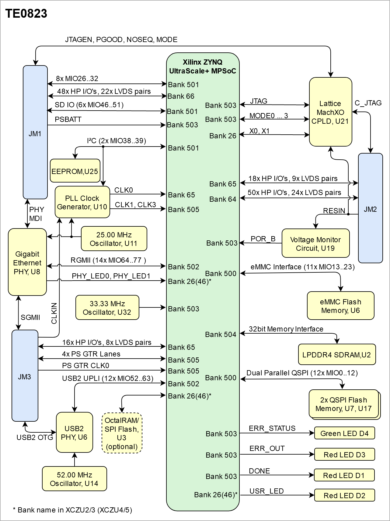
BlockDiagram
| Page properties |
|---|
|
add drawIO object here.
|
| Scroll Title |
|---|
| anchor | Figure_OV_BD |
|---|
| title | TE0823 block diagram |
|---|
|
| Scroll Ignore |
|---|
| scroll-pdf | true |
|---|
| scroll-office | true |
|---|
| scroll-chm | true |
|---|
| scroll- |
|---|
|
|
title| docbook | true |
|---|
| scroll-eclipsehelp | true |
|---|
| scroll-epub | true |
|---|
| scroll-html | true |
|---|
|
|
| anchor | Figure_OV_BD |
|---|
| title | TE0823 block diagram |
|---|
|
scroll-ignore | | draw.io Diagram |
|---|
| border | false |
|---|
| |
|---|
| diagramName | TE0823_OV_BD |
|---|
| simpleViewer | false |
|---|
| width | |
|---|
| links | auto |
|---|
| tbstyle | hidden |
|---|
| diagramDisplayName | |
|---|
| lbox | true |
|---|
| diagramWidth | 641 |
|---|
| revision | 1116 |
|---|
|
|
| Scroll Only |
|---|
|
|
Main Components
...
| Scroll Title |
|---|
| anchor | Table_OV_BP |
|---|
| title | Boot process. |
|---|
|
| Scroll Table Layout |
|---|
| orientation | portrait |
|---|
| sortDirection | ASC |
|---|
| repeatTableHeaders | default |
|---|
| style | |
|---|
| widths | |
|---|
| sortByColumn | 1 |
|---|
| sortEnabled | false |
|---|
| cellHighlighting | true |
|---|
|
MODE Signal State | Boot Mode |
|---|
| LowHigh | QSPI* | | HighLow | SD Card* |
*changable also with other CPLD Firmware:TE0823 CPLD |
| Scroll Title |
|---|
| anchor | Table_OV_RST |
|---|
| title | Reset process. |
|---|
|
| Scroll Table Layout |
|---|
| orientation | portrait |
|---|
| sortDirection | ASC |
|---|
| repeatTableHeaders | default |
|---|
| style | |
|---|
| widths | |
|---|
| sortByColumn | 1 |
|---|
| sortEnabled | false |
|---|
| cellHighlighting | true |
|---|
|
Signal | B2B | I/O | Note |
|---|
ENRESIN | JM1JM2-2818 | InputCPLD Enable Pin |
|
|
Signals, Interfaces and Pins
...
| Scroll Title |
|---|
| anchor | Table_SIP_TPs |
|---|
| title | Test Points Information |
|---|
|
| Scroll Table Layout |
|---|
| orientation | portrait |
|---|
| sortDirection | ASC |
|---|
| repeatTableHeaders | default |
|---|
| style | |
|---|
| widths | |
|---|
| sortByColumn | 1 |
|---|
| sortEnabled | false |
|---|
| cellHighlighting | true |
|---|
| 1 |
|---|
| sortEnabled | false |
|---|
| cellHighlighting | true |
|---|
|
| Test Point | Signal | Connected to | Notes |
|---|
| 1 | PS_LP0V85 | Regulator, U12 |
| | 2 | SRST |
| Test Point | Signal | Connected to | Notes |
|---|
1 | I2C_SCL | EEPROM, U25 | 2 | I2C_SDA | EEPROM, U25 | | 3 | SRST_B | FPGA Bank 503 | PSCONFIG | | 4 | PS_CLK | FPGA Bank 503 | PSCONFIG | | 5 | PROG_B | FPGA Bank 503 | PSCONFIG | 6 | INIT8| _B | FPGA Bank 503, U1H | PSCONFIG |
7 | DONE | Red LED, D1 | LP0V85Voltage U129 | DDR_2V5 | Voltage Regulator, U4 |
| | 4 | +1.1V_LPDDR4 | Regulator, U15 |
| | 5 |
10AVCCVoltage U911DDR_1V2 | Voltage Regulator, U15 | 12AVTTVoltage U313FP0V85 U2614 Translator15
| | 10 | PS_PLL | Voltage Regulator, U23 |
16
| | 11 | PL_VCCINT | Voltage Regulator, U5 |
| | 12...15 | - | - |
| | 16 | PL_VCU | Voltage Regulator, U24 |
|
|
On-board Peripherals
| Page properties |
|---|
|
Notes : - add subsection for every component which is important for design, for example:
- Two 100 Mbit Ethernet Transciever PHY
- USB PHY
- Programmable Clock Generator
- Oscillators
- eMMCs
- RTC
- FTDI
- ...
- DIP-Switches
- Buttons
- LEDs
|
...
The TE0821 is equipped with dual Flash Memory, U7, U17. Two quad SPI compatible serial bus flash MT25QU512ABB8E12-0SIT flash memory chips are provided for FPGA configuration file and data storage. After configuration completes the remaining free memory can be used for application data storage. All four SPI data lines are connected to the FPGA allowing x1, x2 or x4 data bus widths to be used. The maximum data transfer rate depends on the bus width and clock frequency.
...
| Scroll Title |
|---|
| anchor | Table_OBP_SPI |
|---|
| title | Quad SPI interface MIOs and pins |
|---|
|
| Scroll Table Layout |
|---|
| orientation | portrait |
|---|
| sortDirection | ASC |
|---|
| repeatTableHeaders | default |
|---|
| style | |
|---|
| widths | |
|---|
| sortByColumn | 1 |
|---|
| sortEnabled | false |
|---|
| cellHighlighting | true |
|---|
|
MIO | Pin | Schematic | U?? Pin | Notes | | QSPI, U7 | QSPI, U17Notes |
|---|
| nCS | MIO5 | MIO7 |
| | CLK | MIO0 | MIO12 |
| | DI/IO0 | MIO4 | MIO8 |
| | DO/IO1 | MIO1 | MIO9 |
| | nHOLD/IO3 | MIO3 | MIO11 |
| | WP/IO2 | MIO2 | MIO10 |
|
|
EEPROM
There is a 2Kb EEPROM provided on the module TE0821.
| Scroll Title |
|---|
| anchor | Table_OBP_EEP |
|---|
| title | I2C EEPROM interface MIOs and pins |
|---|
|
| Scroll Table Layout |
|---|
| orientation | portrait |
|---|
| sortDirection | ASC |
|---|
| repeatTableHeaders | default |
|---|
| style | |
|---|
| widths | |
|---|
| sortByColumn | 1 |
|---|
| sortEnabled | false |
|---|
| cellHighlighting | true |
|---|
|
| MIO Pin | Schematic | U?? Pin | Notes |
|---|
| MIO39 | I2C_SDA | SDA |
| | MIO38 | I2C_SCL | SCL |
|
|
| Scroll Title |
|---|
| anchor | Table_OBP_I2C_EEPROM |
|---|
| title | I2C address for EEPROM |
|---|
|
| Scroll Table Layout |
|---|
| orientation | portrait |
|---|
| sortDirection | ASC |
|---|
| repeatTableHeaders | default |
|---|
| style | |
|---|
| widths | |
|---|
| sortByColumn | 1 |
|---|
| sortEnabled | false |
|---|
| cellHighlighting | true |
|---|
|
| MIO Pin | I2C Address | Designator | Notes |
|---|
| MIO38-MIO39 | 0x50 | U25 |
|
|
LEDs
| Scroll Title |
|---|
| anchor | Table_OBP_LED |
|---|
| title | On-board LEDs |
|---|
|
| Scroll Table Layout |
|---|
| orientation | portrait |
|---|
| sortDirection | ASC |
|---|
| repeatTableHeaders | default |
|---|
| style | |
|---|
| widths | |
|---|
| sortByColumn | 1 |
|---|
| sortEnabled | false |
|---|
| cellHighlighting | true |
|---|
|
| Designator | Color | Connected to | Active Level | Note |
|---|
| D1 | Red | DONE | Low |
| | D2 | Green | USR_LED | High |
| | D3 | Red | ERR_OUT | High |
| | D4 | Green | ERR_STATUS | High |
|
|
...
| Page properties |
|---|
|
Notes : Minimum and Maximum density of DDR3 SDRAM must be mentioned for other assembly options. (pay attention to supported address length for DDR3) |
The TE0821 TE0823 SoM has dual 8 Gb volatile DDR4 a 1 GB volatile LPDDR4 SDRAM IC for storing user application code and data.
- Part number: K4A8G165WB-BIRC IS43LQ32256A
- Supply voltage: 1.2V7V ~ 1.95V
- Speed: 2400 3200 Mbps
- Temperature: -40 ~ 95 °C
...
Power supply with minimum current capability of xx 2.5 A for system startup is recommended.
...
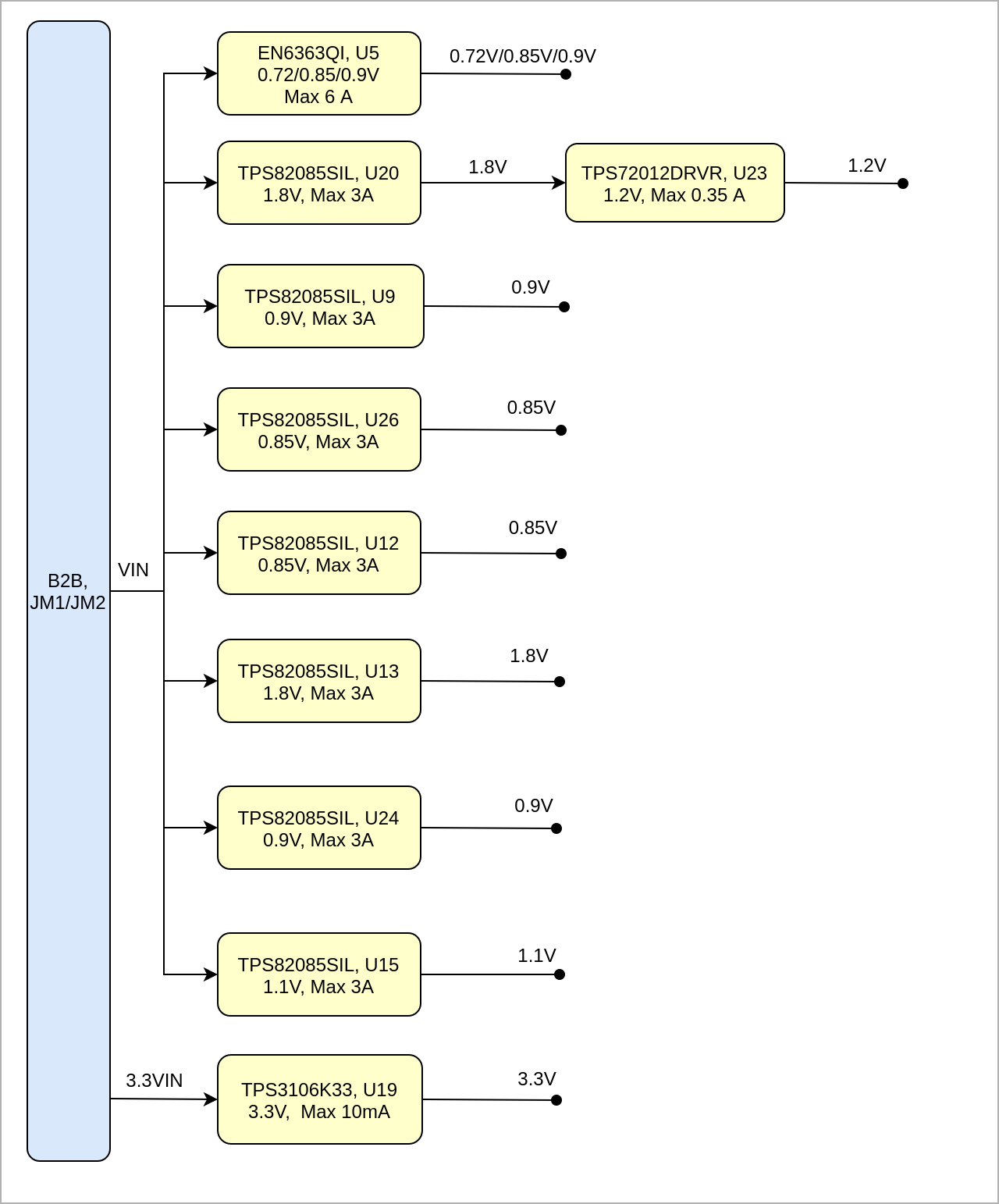
| Scroll Title |
|---|
| anchor | Figure_PWR_PD |
|---|
| title | Power Distribution |
|---|
|
| Scroll Ignore |
|---|
| draw.io Diagram |
|---|
| border | false |
|---|
| |
|---|
| diagramName | TE0823_PWR_PD |
|---|
| simpleViewer | false |
|---|
| width | |
|---|
| links | auto |
|---|
| tbstyle | hidden |
|---|
| diagramDisplayName | |
|---|
| lbox | true |
|---|
| diagramWidth |
|---|
|
6414
|
| Scroll Only |
|---|
|
|
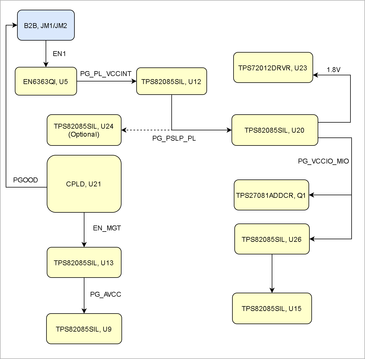
Power-On Sequence
| Scroll Title |
|---|
| anchor | Figure_PWR_PS |
|---|
| title | Power Sequency |
|---|
|
| Scroll Ignore |
|---|
| draw.io Diagram |
|---|
| border | false |
|---|
| |
|---|
| diagramName | TE0823_PWR_PS |
|---|
| simpleViewer | false |
|---|
| width | |
|---|
| links | auto |
|---|
| tbstyle | hidden |
|---|
| diagramDisplayName | |
|---|
| lbox | true |
|---|
| diagramWidth | 641640 |
|---|
| revision | 36 |
|---|
|
|
| Scroll Only |
|---|
|
|
Power Rails
| Scroll Title |
|---|
| anchor | Table_PWR_PR |
|---|
| title | Module power rails. |
|---|
|
| Scroll Table Layout |
|---|
| orientation | portrait |
|---|
| sortDirection | ASC |
|---|
| repeatTableHeaders | default |
|---|
| style | |
|---|
| widths | |
|---|
| sortByColumn | 1 |
|---|
| sortEnabled | false |
|---|
| cellHighlighting | true |
|---|
|
| Power Rail Name | B2B Connector JM1 Pin | B2B Connector JM2 Pin | B2B Connector JM3 Pin | Direction | Notes |
|---|
| VIN | 1, 3, 5 | 2, 4, 6, 8 | Input | Supply voltage from the carrier board |
| | 3.3V | - | 10, 12 | Output | Internal 3.3V voltage level |
| | 3.3VIN | 13, 15 | - | Input | Supply voltage from the carrier board |
| | 1.8V | 39 | - | Output | Internal 1.8V voltage level |
| | JTAG VREF | - | 91 | Output | JTAG reference voltage.
Attention: Net name on schematic is "3.3VIN" |
| | VCCO_64 | - | 7, 9 | Input | High performance I/O bank voltage |
| | VCCO_65 | - | 5 | Input | High performance I/O bank voltage |
| | VCCO_66 | 9, 11 | - | Input | High performance I/O bank voltage |
|
|
...
| Page properties |
|---|
|
- This section is optional and only for modules.
use "include page" macro and link to the general B2B connector page of the module series, For example: 6 x 6 SoM LSHM B2B Connectors
| Include Page |
|---|
| PD:6 x 6 SoM LSHM B2B ConnectorsPD: |
|---|
| 6 x 6 SoM LSHM B2B Connectors |
|---|
|
|
| Include Page |
|---|
| PD:4 x 5 SoM LSHM B2B ConnectorsPD: |
|---|
| 4 x 5 SoM LSHM B2B Connectors |
|---|
|
...
| Scroll Title |
|---|
| anchor | Table_TS_ROC |
|---|
| title | Recommended operating conditions. |
|---|
|
| Scroll Table Layout |
|---|
| orientation | portrait |
|---|
| sortDirection | ASC |
|---|
| repeatTableHeaders | default |
|---|
| style | |
|---|
| widths | |
|---|
| sortByColumn | 1 |
|---|
| sortEnabled | false |
|---|
| cellHighlighting | true |
|---|
|
| Parameter | Min | Max | Units | Reference Document |
|---|
| VIN supply voltage | 3.3 | 6 | V | See TPS82085S datasheet | | 3.3VIN supply voltage | 3.3 | 3.465 | V | See LCMXO2-256HC, Xilinx DS925 datasheet | | PS I/O supply voltage, VCCO_PSIO | 1.710 | 3.465 | V | Xilinx document DS925 | | PS I/O input voltage | –0.20 | VCCO_PSIO + 0.20 | V | Xilinx document DS925 | | HP I/O banks supply voltage, VCCO | 0.950 | 1.9 | V | Xilinx document DS925 | | HP I/O banks input voltage | -0.20 | VCCO + 0.20 | V | Xilinx document DS925 | | Voltage on SC CPLD pins | -0.3 | 3.6 | V | Lattice Semiconductor MachXO2 datasheet | | Operating Temperature Range | 0 | 85 | °C | Xilinx document DS925, extended grade Zynq temperarure range |
|
...
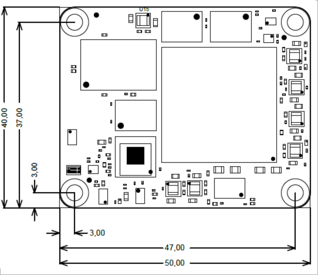
| Scroll Title |
|---|
| anchor | Figure_TS_PD |
|---|
| title | Physical Dimension |
|---|
|
| Scroll Ignore |
|---|
| draw.io Diagram |
|---|
| border | false |
|---|
| |
|---|
| diagramName | TE0823_TS_PD |
|---|
| simpleViewer | false |
|---|
| width | |
|---|
| links | auto |
|---|
| tbstyle | hidden |
|---|
| diagramDisplayName | |
|---|
| lbox | true |
|---|
| diagramWidth | 542 |
|---|
| revision | 34 |
|---|
|
|
| Scroll Only |
|---|
| scroll-pdf | true |
|---|
| scroll-office | true |
|---|
| scroll-chm | true |
|---|
| scroll-docbook | true |
|---|
| scroll-eclipsehelp | true |
|---|
| scroll-epub | true |
|---|
| scroll-html | true |
|---|
| 
|
|
...
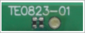
| Scroll Title |
|---|
| anchor | Figure_RV_HRN |
|---|
| title | Board hardware revision number. |
|---|
|
| Scroll Ignore |
|---|
| scroll-pdf | true |
|---|
| scroll-office | true |
|---|
| scroll-chm | true |
|---|
| scroll-docbook | true |
|---|
| scroll-eclipsehelp | true |
|---|
| scroll-epub | true |
|---|
| scroll-html | true |
|---|
| | draw.io Diagram |
|---|
| border | false |
|---|
| |
|---|
| diagramName | TE0823_RV_HRN |
|---|
| simpleViewer | false |
|---|
| width | |
|---|
| links | auto |
|---|
| tbstyle | hidden |
|---|
| diagramDisplayName | |
|---|
| lbox | true |
|---|
| diagramWidth | 170 |
|---|
| revision | 2 |
|---|
|
|
| Scroll Only |
|---|
|
|
...
| Scroll Title |
|---|
| anchor | Table_RH_DCH |
|---|
| title | Document change history. |
|---|
|
| Scroll Table Layout |
|---|
| orientation | portrait |
|---|
| sortDirection | ASC |
|---|
| repeatTableHeaders | default |
|---|
| style | |
|---|
| widths | |
|---|
| sortByColumn | 1 |
|---|
| sortEnabled | false |
|---|
| cellHighlighting | true |
|---|
|
| Date | Revision | Contributor | Description |
|---|
| Page info |
|---|
| infoType | Modified date |
|---|
| dateFormat | yyyy-MM-dd |
|---|
| type | Flat |
|---|
|
| | Page info |
|---|
| infoType | Current version |
|---|
| prefix | v. |
|---|
| type | Flat |
|---|
| showVersions | false |
|---|
|
| | Page info |
|---|
| infoType | Modified by |
|---|
| type | Flat |
|---|
| showVersions | false |
|---|
|
| | | 2021-08-23 | v.42 | Pedram Babakhani | | | 2020-11-02 | v.40 | Pedram Babakhani | | -- | all | | Page info |
|---|
| infoType | Modified users |
|---|
| type | Flat |
|---|
| showVersions | false |
|---|
|
| |
|
...