...
| Scroll Title |
|---|
| anchor | Figure_OV_BD |
|---|
| title | TE0823 block diagram |
|---|
|
| Scroll Ignore |
|---|
| draw.io Diagram |
|---|
| border | false |
|---|
| |
|---|
| diagramName | TE0823_OV_BD |
|---|
| simpleViewer | false |
|---|
| width | |
|---|
| links | auto |
|---|
| tbstyle | hidden |
|---|
| diagramDisplayName | |
|---|
| lbox | true |
|---|
| diagramWidth | 641 |
|---|
| revision | 56 |
|---|
|
|
| Scroll Only |
|---|
|
|
Main Components
...
| Scroll Title |
|---|
| anchor | Table_OV_IDS |
|---|
| title | Initial delivery state of programmable devices on the module |
|---|
|
| Scroll Table Layout |
|---|
| orientation | portrait |
|---|
| sortDirection | ASC |
|---|
| repeatTableHeaders | default |
|---|
| style | |
|---|
| widths | |
|---|
| sortByColumn | 1 |
|---|
| sortEnabled | false |
|---|
| cellHighlighting | true |
|---|
|
Storage device name | Content | Notes |
|---|
Quad SPI QSPI Flash | EEPROM | Memory | Not programmed |
| eMMC Memory | Not programmed |
| | Programmable Clock Generator | Not programmed |
| | CPLD (LCMXO2-256HC) | SC0820-02 QSPI FirmwareSystem Controller CPLD |
|
|
Configuration Signals
| Page properties |
|---|
|
- Overview of Boot Mode, Reset, Enables.
|
...
| Scroll Title |
|---|
| anchor | Table_OV_BP |
|---|
| title | Boot process. |
|---|
|
| Scroll Table Layout |
|---|
| orientation | portrait |
|---|
| sortDirection | ASC |
|---|
| repeatTableHeaders | default |
|---|
| style | |
|---|
| widths | |
|---|
| sortByColumn | 1 |
|---|
| sortEnabled | false |
|---|
| cellHighlighting | true |
|---|
|
MODE Signal State | Boot Mode |
|---|
| Low | QSPI | | High | SD Card |
|
| Scroll Title |
|---|
| anchor | Table_OV_RST |
|---|
| title | Reset process. |
|---|
|
| Scroll Table Layout |
|---|
| orientation | portrait |
|---|
| sortDirection | ASC |
|---|
| repeatTableHeaders | default |
|---|
| style | |
|---|
| widths | |
|---|
| sortByColumn | 1 |
|---|
| sortEnabled | false |
|---|
| cellHighlighting | true |
|---|
|
|
...
| Scroll Title |
|---|
| anchor | Table_SIP_B2B |
|---|
| title | General PL I/O to B2B connectors information |
|---|
|
| Scroll Table Layout |
|---|
| orientation | portrait |
|---|
| sortDirection | ASC |
|---|
| repeatTableHeaders | default |
|---|
| style | |
|---|
| widths | |
|---|
| sortByColumn | 1 |
|---|
| sortEnabled | false |
|---|
| cellHighlighting | true |
|---|
|
| FPGA Bank | B2B Connector | I/O Signal Count | Voltage Level | Notes |
|---|
|
...
JTAG access to the TExxxx SoM through B2B connector JMX.
...
| anchor | Table_SIP_JTG |
|---|
| title | JTAG pins connection |
|---|
|
|---|
| 24 | HD | JM2 | 24x I/O, 12x LVDS Pairs | Variable | Max voltage 3.3V | | 25 | HD | JM1 | 24x I/O, 12x LVDS Pairs | Variable | Max voltage 3.3V | | 26 | HD | JM1 | 24x I/O, 12x LVDS Pairs | Variable | Max voltage 3.3V | | 44 | HD | JM2 | 24x I/O, 12x LVDS Pairs | Variable | Max voltage 3.3V | | 65 | HP | JM2 | 18x I/O, 9x LVDS Pairs | Variable | Max voltage 1.8V | 65 | HP | JM3 | 16x I/O, 8x LVDS Pairs | Variable | Max voltage 1.8V | | 505 | GTR | JM3 | 16x I/O, 8x LVDS Pairs | - | 4x lanes | | 505 | GTR CLK | JM3 | 1x Diff Clock | - |
| 501 | MIO | JM1 | 15 I/O | 3.3V |
|
|
JTAG Interface
JTAG access to the Xilinx Zynq UltraScale+ is applicable by using Lattice MachXO CPLD through B2B connector JM2.
| Scroll Title |
|---|
| anchor | Table_SIP_JTG |
|---|
| title | JTAG pins connection |
|---|
|
| Scroll Table Layout |
|---|
| orientation | portrait |
|---|
| sortDirection | ASC |
|---|
| repeatTableHeaders | default |
|---|
| style | |
|---|
| widths | |
|---|
| sortByColumn | 1 |
|---|
| sortEnabled | false |
|---|
| cellHighlighting | true |
|---|
|
JTAG Signal | B2B Connector | Notes |
|---|
| TMS | JM2-93 |
| | TDI | JM2-95 |
| | TDO | JM2-97 |
| | TCK | JM2-99 |
| | JTAGEN | JM1-89 | Pulled Low: Xilinx Zynq UltraScale+ MPSoC
Pulled High: Lattice MachXO CPLD |
|
MGT Lanes
There are 4x MGT Lanes connected to FPGA Bank 505-GTR.
| Scroll Title |
|---|
| anchor | Table_SIP_MGT |
|---|
| title | MGT Lanes connection |
|---|
|
| Scroll Table Layout |
|---|
| orientation | portrait |
|---|
| sortDirection | ASC |
|---|
| repeatTableHeaders | default |
|---|
| style | |
|---|
| widths | |
|---|
| sortByColumn | 1 |
|---|
| sortEnabled | false |
|---|
| cellHighlighting | true |
|---|
|
Lane | Schematic | B2B | Note |
|---|
| 0 | - B505_RX0_P
- B505_RX0_N
- B505_TX0_P
- B505_TX0_N
| |
| | 1 | - B505_RX1_P
- B505_RX1_N
- B505_TX1_P
- B505_TX1_N
| |
| | 2 | - B505_RX2_P
- B505_RX2_N
- B505_TX2_P
- B505_TX2_N
| |
| | 3 | - B505_RX2_P
- B505_RX2_N
- B505_TX2_P
- B505_TX2_N
| |
|
|
Gigabit Ethernet
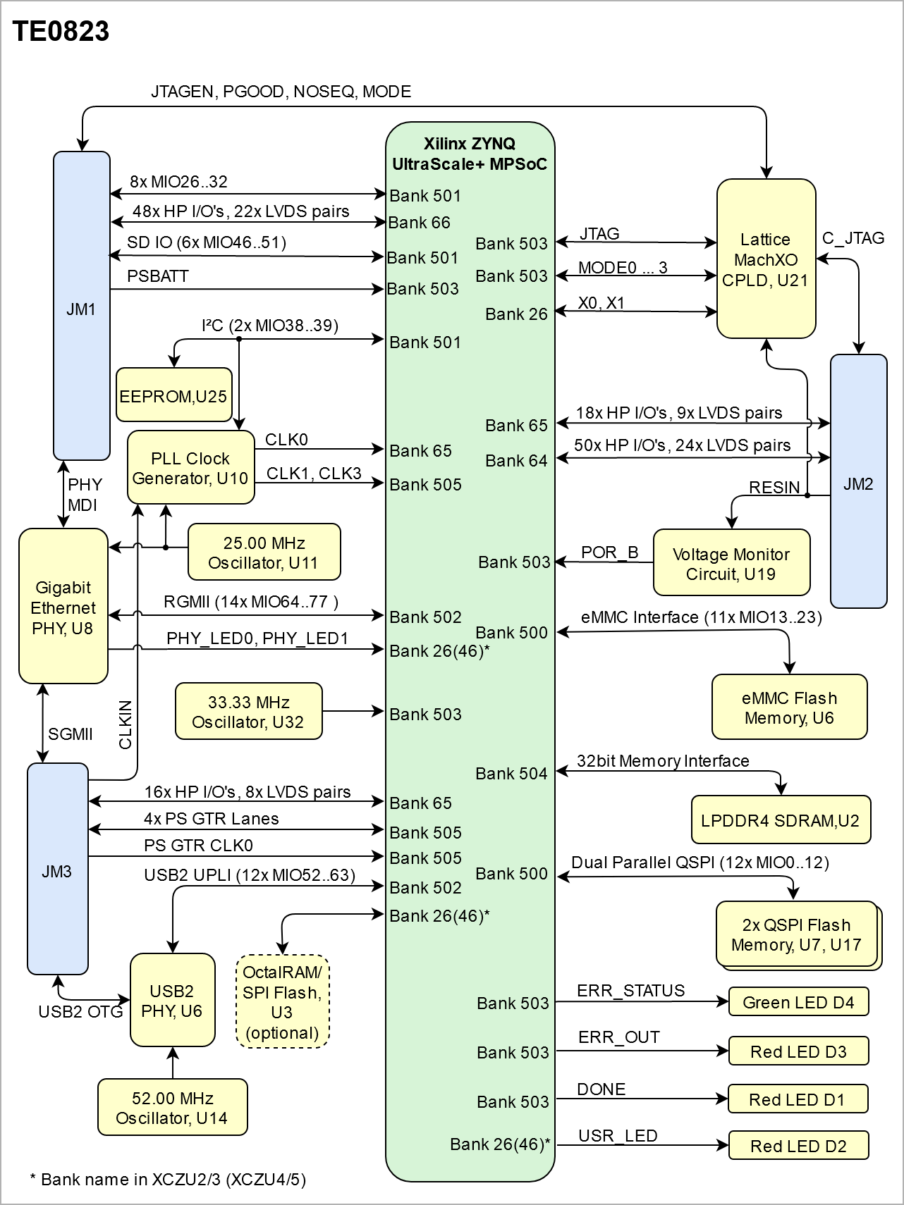
On-board Gigabit Ethernet PHY is provided with Marvell Alaska 88E1512 chip. The Ethernet PHY RGMII interface is connected to the Zynq Ethernet0 PS GEM0. I/O voltage is fixed at 1.8V for HSTL signaling. SGMII (SFP copper or fiber) can be used directly with the Ethernet PHY, as the SGMII pins are available on the B2B connector JM3. The reference clock input of the PHY is supplied from an on-board 25MHz oscillator (U11), the 125MHz output clock is left unconnected.
| Scroll Title |
|---|
| anchor | Table_SIP_ETH |
|---|
| title | GigaBit Ethernet connection |
|---|
|
| Scroll Table Layout |
|---|
| orientation | portrait |
|---|
| sortDirection | ASC |
|---|
| repeatTableHeaders | default |
|---|
| style | |
|---|
| widths | |
|---|
| sortByColumn | 1 |
|---|
| sortEnabled | false |
|---|
| cellHighlighting | true |
|---|
|
| Pin | Schematic | Connected to | Note |
|---|
| MDIP0...3 | PHY_MDI0...3 | B2B, JM1 |
| | MDC | ETH_MDC | MIO76 |
| | MDIO | ETH_MDIO | MIO77 |
| | S_IN | S_IN | B2B, JM3 |
| | S_OUT | S_OUT | B2B, JM3 |
| | TXD0..3 | ETH_TXD0...3 | MIO65...68 |
| | TX_CTRL | ETH_TXCTL | MIO69 |
| | TX_CLK | ETH_TXCK | MIO64 |
| | RXD0...3 | ETH_RXD0...3 | MIO71...74 |
| | RX_CTRL | ETH_RXCTL | MIO75 |
| | RX_CLK | ETH_RXCK | MIO70 |
| | LED0...2 | PHY_LED0...2 | FPGA Bank 66 |
| | RESETn | ETH_RST | MIO24 |
|
|
System Controller CPLD
Special purpose pins are connected to System Controller CPLD and have following default configuration:
| Scroll Title |
|---|
| anchor | Table_SIP_CPLD |
|---|
| title | System Controller CPLD special purpose pins |
|---|
|
| Scroll Table Layout |
|---|
| orientation | portrait |
|---|
| sortDirection | ASC |
|---|
| repeatTableHeaders | default |
|---|
| style | |
|---|
| widths | |
|---|
| sortByColumn | 1 |
|---|
| sortEnabled | false |
|---|
| cellHighlighting | true |
|---|
|
| Pin Name | Mode | Function | Default Configuration |
|---|
| EN1 | Input | Power Enable | No hard wired function on PCB. When forced low, PGOOD goes low without effect on power management | | PGOOD | Output | Power Good | Only indirect used for power status, see CPLD description | | NOSEQ | - | - | No used for Power sequencing, see CPLD description | | RESIN | Input | Reset | Active low reset, gated to POR_B | | JTAGEN | Input | JTAG Select | Low for normal operation, high for CPLD JTAG access |
|
USB Interface
USB PHY is provided by Microchip USB3320. The ULPI interface is connected to the Zynq PS USB0. I/O voltage is fixed at 1.8V. Reference clock input for the USB PHY is supplied by the on-board 52.00 MHz oscillator (U14).
| Scroll Title |
|---|
| anchor | Table_SIP_USB |
|---|
| title | General overview of the USB PHY signals |
|---|
|
| Scroll Table Layout |
|---|
| orientation | portrait |
|---|
| sortDirection | ASC |
|---|
| repeatTableHeaders | default |
|---|
| style | |
|---|
| widths | |
|---|
| sortByColumn | 1 |
|---|
| sortEnabled | false |
|---|
| cellHighlighting | true |
|---|
|
| PHY Pin | ZYNQ Pin | B2B Name | Notes |
|---|
| ULPI | MIO52..63 | - | Zynq USB0 MIO pins are connected to the USB PHY. | | REFCLK | - | - | 52.000000 MHz from on-board oscillator (U14). | | REFSEL[0..2] | - | - | Reference clock frequency select, all set to GND selects 52.000000 MHz. | | RESETB | MIO25 | - | Active low reset. | | CLKOUT | MIO52 | - | Connected to 1.8V, selects reference clock operation mode. | | DP, DM | - | OTG_D_P, OTG_D_N | USB data lines routed to B2B connector JM3 pins 47 and 49. | | CPEN | - | VBUS_V_EN | External USB power switch active high enable signal, routed to JM3 pin 17. | | VBUS | - | USB_VBUS | Connect to USB VBUS via a series of resistors, see reference schematics, routed to JM3 pin 55. | | ID | - | OTG_ID | For an A-device connect to ground, for a B-device left floating. routed from JM3 pin 23. |
|
MIO Pins
| Page properties |
|---|
|
you must fill the table below with group of MIOs which are connected to a specific components or peripherals, you do not have to specify pins in B2B, Just mention which B2B is connected to MIOs. The rest is clear in the Schematic. Example: | MIO Pin | Connected to | B2B | Notes |
|---|
| MIO12...14 | SPI_CS , SPI_DQ0... SPI_DQ3 SPI_SCK | J2 | QSPI |
|
| Scroll Title |
|---|
| anchor | Table_SIP_MIOs |
|---|
| title | MIOs pins |
|---|
|
| Scroll Table Layout |
|---|
| orientation | portrait |
|---|
| sortDirection | ASC |
|---|
| repeatTableHeaders | default |
|---|
| style | |
|---|
| widths | |
|---|
| sortByColumn | 1 |
|---|
| sortEnabled | false |
|---|
| cellHighlighting | true |
|---|
|
| MIO Pin | Connected to | B2B | Notes |
|---|
| 0...5 | QSPI Flash, U7 | - | SPI Flash | | 7...12 | QSPI Flash, U17 | - | SPI Flash | | 13...23 | eMMC, U6 |
|
| | 24 | ETH Transceiver, U8 | - | ETH_RST | | 25 | USB2.0 Transceiver, U18 | - | OTG_RST | | 26...33 | User MIO | JM1 |
| | 34...37 | N.C | - | N.C | | 38...39 | EEPROM, U25 | - | I2C_SDA/SCL | | 40...45 | N.C |
| N.C | | 46...51 | SD Card | JM1 |
| | 52...63 | USB2.0 Transceiver, U18 | - |
| | 63...77 | Ethernet Transceiver, U8 | - |
|
|
Test Points
...
JTAG Signal
...
B2B Connector
...
| Page properties |
|---|
|
you must fill the table below with group of MIOs Test Point which are connected to a specific components or peripherals, you do not have to specify pins in B2B, Just mention which B2B is connected to MIOs. The rest is clear in the Schematicindicated as TP in a schematic. If there is no Test Point remarked in the schematic, delet the Test Point section. Example: | Test Point | Signal | MIO Pin | Connected to | B2B | Notes |
|---|
| MIO12...14 | SPI_CS , SPI_DQ0... SPI_DQ3 SPI_SCK | J2 | QSPI | | 10 | PWR_PL_OK | J2-120 |
|
|
| Scroll Title |
|---|
| anchor | Table_SIP_MIOsTPs |
|---|
| title | MIOs pinsTest Points Information |
|---|
|
| Scroll Table Layout |
|---|
| orientation | portrait |
|---|
| sortDirection | ASC |
|---|
| repeatTableHeaders | default |
|---|
| style | |
|---|
| widths | |
|---|
| sortByColumn | 1 |
|---|
| sortEnabled | false |
|---|
| cellHighlighting | true |
|---|
|
|
Test Points
| Notes |
|---|
| 1 | I2C_SCL | EEPROM, U25 |
| | 2 | I2C_SDA | EEPROM, U25 |
| | 3 | SRST_B | FPGA Bank 503 | PSCONFIG | | 4 | PS_CLK | FPGA Bank 503 | PSCONFIG | | 5 | PROG_B | FPGA Bank 503 | PSCONFIG | | 6 | INIT_B | FPGA Bank 503 | PSCONFIG | | 7 | DONE | Red LED, D1 |
| | 8 | PS_LP0V85 | Voltage Regulator, U12 |
| | 9 | DDR_2V5 | Voltage Regulator, U4 |
| | 10 | PS_AVCC | Voltage Regulator, U9 |
| | 11 | DDR_1V2 | Voltage Regulator, U15 |
| | 12 | PS_AVTT | Voltage Regulator, U3 |
| | 13 | PS_FP0V85 | Voltage Regulator, U26 |
| | 14 | POR_B | Voltage Translator, U19 |
| | 15 | PS_PLL | Voltage Regulator, U23 |
| | 16 | PL_VCCINT | Voltage Regulator, U5 |
|
| Page properties |
|---|
|
you must fill the table below with group of Test Point which are indicated as TP in a schematic. If there is no Test Point remarked in the schematic, delet the Test Point section.
Example:
| Test Point | Signal | B2B | Notes |
|---|
10 | PWR_PL_OK | J2-120 | | Scroll Title |
|---|
| anchor | Table_SIP_TPs |
|---|
| title | Test Points Information |
|---|
|
| Scroll Table Layout |
|---|
|
| orientation | portrait |
|---|
| sortDirection | ASC |
|---|
| repeatTableHeaders | default |
|---|
style | widths | | sortByColumn | 1 |
|---|
| sortEnabled | false |
|---|
| cellHighlighting | true |
|---|
| Test Point | Signal | Connected to | Notes
On-board Peripherals
| Page properties |
|---|
|
Notes : - add subsection for every component which is important for design, for example:
- Two 100 Mbit Ethernet Transciever PHY
- USB PHY
- Programmable Clock Generator
- Oscillators
- eMMCs
- RTC
- FTDI
- ...
- DIP-Switches
- Buttons
- LEDs
|
...