Table of Contents
Overview
The Trenz Electronic TEBF0808 Carrier Board is a baseboard for the Xilinx Zynq Ultrascale+ MPSoC modules TE0808 and TE0803, which exposes the module's B2B connector pins to accessible connectors and provides a whole range of on-board components to test and evaluate the Zynq Ultrascale+ SoMs and for developing purposes.
Key Features
- Mini-ITX form factor, PC Enclosure compatible
- ATX power supply connector
- Optional 12V standard power plug
- Headers
- Intel 10-pin HDA Audio
- Intel 9-pin Power-/Reset-Button, Power-/HD-LED
- PC-BEEPER
- On-board Power- / Reset-Switches
- 2x Configuration 4-bit DIP-switches
- 2x Optional 4-wire PWM fan connectors
- PCIe Slot - one PCIe lane (16 lane connector)
- CAN FD Transceiver (10 Pin IDC connector and 6-pin header)
- 4x On-board configuration EEPROMs (1x Microchip 24LC128-I/ST, 3x Microchip 24AA025E48T-I/OT)
- Dual SFP+ Connector (2x1 Cage)
- One Display-Port (single lane)
- One SATA Connector
- 2x USB3.0 A Connector (Superspeed Host Port (Highspeed at USB2.0))
- 1x USB3.0 on-board header with two ports
- FMC HPC Slot (FMC_VADJ max. VCCIO)
- FMC Fan
- Gigabit Ethernet RGMII PHY with RJ45 MegJack
- All Carrier Board peripherals' I²C-interfaces muxed to MPSoC's I²C-interface on PS bank 503
- Quad programmable PLL clock generator SI5338A
- 2x SMA coaxial connectors for clock signals
- MicroSD- / MMC-Card Socket (bootable)
- 32 Gbit on-board eMMC memory (8 banks a 4 Gbit)
- Two System Controller CPLDs Lattice MachXO2 1200 HC
- One Samtec FireFly (4 GT lanes bidirectional)
- One Samtec FireFly connector for reverse loopback
- 2x JTAG/UART header ('XMOD FTDI JTAG Adapter'-compatible) for programming MPSoC and SC CPLDs
- 20 Pin ARM JTAG Connector (PS JTAG0)
- 3x PMOD connector (GPIO's and I²C interface to SC CPLDs / MPSoC module
- Carrier SC CPLD managing power-up sequence of MPSoC module
- On-board DCDC PowerSoCs
Additional assembly options are available for cost or performance optimization upon request.
Block Diagram
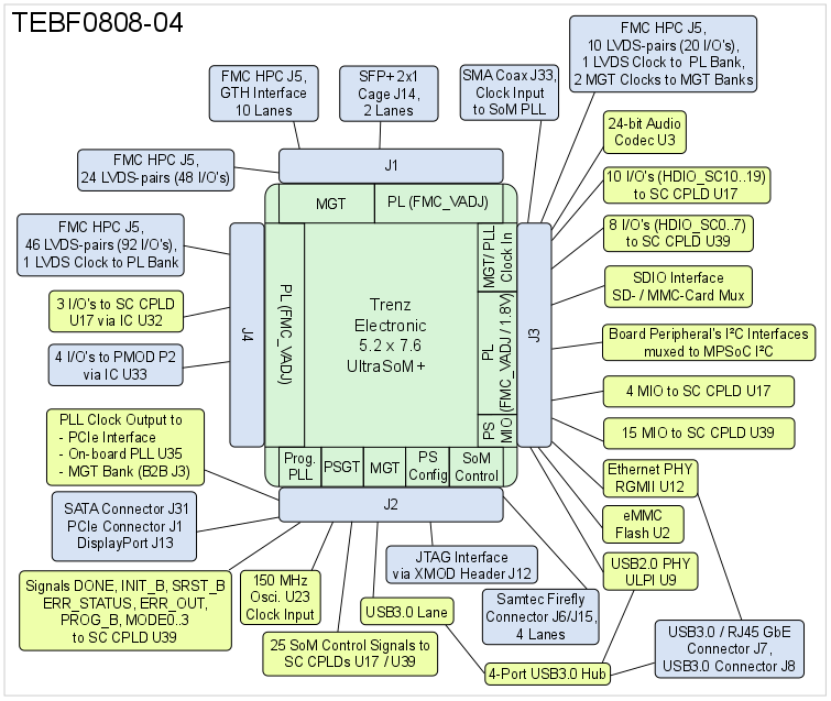
Figure 1: TEBF0808-04 Block Diagram
Main Components
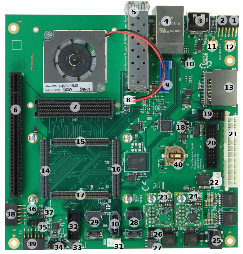
Figure 2: TEBF0808-04 Carrier Board
- PMOD connector, P2
- MicroSD Card socket (on bottom side), J16
- Display Port socket, J13
- USB3.0 A 2x , RJ45 1x (stacked), J7
- SFP+ 2x1 cage, J14
- PCIe x16 connector (one PCIe lane connected), J11
- FMC HPC, J5
- FMC-Fan connector 5V, J19
- USB3.0 connector, J8
- PC-BEEPER 4-pin header, J23
- SMA coaxial connector (SI5338A clock output), J32
- SMA coaxial connector (clock input to MPSoC module), J33
- eMMC Card socket, J27
- Ultra fine 0.50 mm pitch, Razor Beam™ LP Slim Terminal Strip with 160 contacts, J4
- Ultra fine 0.50 mm pitch, Razor Beam™ LP Slim Terminal Strip with 160 contacts, J1
- Ultra fine 0.50 mm pitch, Razor Beam™ LP Slim Terminal Strip with 160 contacts, J3
- Ultra fine 0.50 mm pitch, Razor Beam™ LP Slim Terminal Strip with 160 contacts, J2
- CAN bus 6-pin header, J29
- CAN bus 10-pin connector, J24
- ARM-JTAG 20-pin connector, J30
- ATX power supply connector, J20
- 4-Wire PWM fan connector, J35
- JTAG/UART header ('XMOD FTDI JTAG Adapter'-compatible) for access to MPSoC module, J12
- JTAG/UART header ('XMOD FTDI JTAG Adapter'-compatible) for access to System Controller CPLDs, J28
- Power Jack 2.1mm 12V, J25
- 4-bit DIP-switch, S5
- Power Button, S1
- Samtec FireFly Connector for reverse loopback, J21/J22
- Samtec FireFly Connector (4 GT lanes bidirectional), J6/J15
- SATA Header, J31
- 4-Wire PWM fan connector, J26
- Programmable on-module PLL I²C interface 10-pin header, J17
- Reset Button, S2
- INTEL HDA 9-pin header, J9
- Intel front panel (PWR-/RST-Button, HD-/PWR-LED) 9-pin header, J10
- Samtec FireFly Connector J6/J15 I²C interface 3-pin header, J34
- 4-bit DIP-switch, S4
- PMOD connector, P3
- PMOD connector, P1
- Battery Holder CR1220, B1
Initial Delivery State
Storage device name | Content | Notes |
|---|---|---|
General Purpose Configuration EEPROMs (1x Microchip 24LC128-I/ST, 3x Microchip 24AA025E48T-I/OT) | Not programmed | - |
| USB3.0 HUB Configuration EEPROM (Microchip 24LC128-I/ST) | Not programmed | - |
| Si5338A programmable PLL NVM OTP | Not programmed | - |
Table 1: Initial Delivery State of the flash memories
Signals, Interfaces and Pins
FMC HPC Connector
The FMC (FPGA Mezzanine Card) connector J5 with high pin count (HPC) provides as an ANSI/VITA 57.1 standard a modular interface to the MPSoCs FPGA and exposes numerous of its I/O pins for use by other mezzanine modules and expansion cards.
The connector supports single ended (VCCIO: FMC_VADJ) and differential signaling as the I/O's are usable as LVDS-pairs.
The I/O signals are routed from the FPGA banks as LVDS-pairs to the connector.
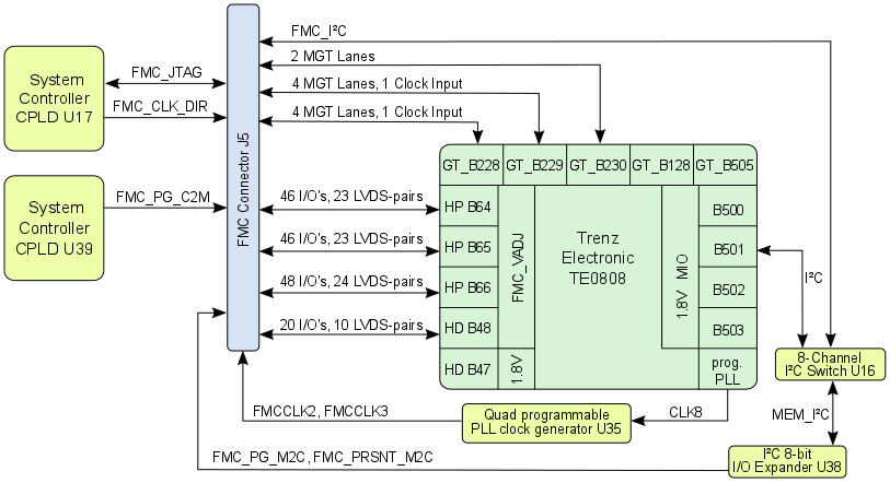
Figure 2: FMC HPC Connector
| FPGA Bank | I/O Signal Count | LVDS-pairs count | VCCO bank Voltage | Reference Clock Input from FMC Connector | Notes |
|---|---|---|---|---|---|
| Bank 48 | 20 | 10 | FMC_VADJ | 1 reference clock signal from FMC connector | - |
| Bank 64 | 46 | 23 | FMC_VADJ | 1 reference clock signal from FMC connector | bank's VREF-pin connected to FMC connector pin J5-H1 (VREF_A_M2C) |
| Bank 65 | 46 | 23 | FMC_VADJ | - | bank's VREF-pin connected to FMC connector pin J5-H1 (VREF_A_M2C) |
| Bank 66 | 48 | 24 | FMC_VADJ | - | bank's VREF-pin connected to FMC connector pin J5-H1 (VREF_A_M2C) |
Table 2: FMC connector pin-outs of available logic banks of the MPSoC
The MGT-banks have also clock input-pins which are exposed to the FMC connector. Following MGT-lanes are available on the FMC connectors J5:
| GT Bank | Type | Count of MGT Lanes | Schematic Names / Connector Pins | MGT Bank's Reference Clock Inputs from FMC Connector |
|---|---|---|---|---|
| 228 | GTH | 4 GTH lanes | B228_RX3_P, B228_RX3_N, pins J5-A10, J5-A11 B228_RX2_P, B228_RX2_N, pins J5-A6, J5-A7 B228_RX1_P, B228_RX1_N, pins J5-A2, J5-A3 B228_RX0_P, B228_RX0_N, pins J5-C6, J5-C7 | 1 reference clock signal (B228_CLK0) from FMC connector |
| 229 | GTH | 4 GTH lanes | B229_RX3_P, B229_RX3_N, pins J5-B12, J5-B13 B229_RX2_P, B229_RX2_N, pins J5-B16, J5-B17 B229_RX1_P, B229_RX1_N, pins J5-A18, J5-A19 B229_RX0_P, B229_RX0_N, pins J5-A14, J5-A15 | 1 reference clock signal (B229_CLK0) from FMC connector |
| 230 | GTH | 2 GTH lanes | B230_RX1_P, B230_RX1_N, pins J5-B4, J5-B5 B230_RX0_P, B230_RX0_N, pins J5-B8, J5-B9 | - |
Table 2: FMC connector pin-outs of available MGT-lanes of the MPSoC
The FMC connector provides pins for reference clock output to the Mezzanine module and clock input to PL banks of the MPSoC:
| Clock Signal Schematic Name | FMC Connector Pins | Direction | Clock Source | Notes |
|---|---|---|---|---|
| B228_CLK0 | J5-D4 / J5-D5 | in | FMC Connector J5 | clock signal to MGT bank 228 |
| B229_CLK0 | J5-B20 / J5-B21 | in | FMC Connector J5 | clock signal to MGT bank 229 |
| FMCCLK2 | J5-K4 / J5-K5 | out | Carrier Board PLL SI5338A U35, CLK2 | - |
| FMCCLK3 | J5-J2 / J5-J3 | out | Carrier Board PLL SI5338A U35, CLK3 | - |
| B64_L14_P / B64_L14_N | J5-H4 / J5-H5 | in | FMC Connector J5 | bank 64 clock capable pin-pair |
| B48_L6_P / B48_L6_N | J5-G2 / J5-G3 | in | FMC Connector J5 | bank 48 clock capable pin-pair |
Table 3: FMC connector pin-outs for reference clock output
The FMC connector provides further interfaces like 'JTAG' and 'I²C' to the System Controller CPLD:
| Interfaces | I/O Signal Count | Pin schematic Names / FMC Pins | Connected to | Notes |
|---|---|---|---|---|
| JTAG | 5 | FMC_TCK, pin J5-D29 FMC_TMS, pin J5-D33 FMC_TDI, pin J5-D30 FMC_TDO, pin J5- D31 | SC CPLD U17, bank 1 | VCCIO: 3V3SB TRST_L, pin J5-D34 pulled-up to 3V3_PER |
| I²C | 2 | FMC_SCL, pin J5-C30 FMC_SDA, pin J5-C31 | I²C-Switch U16 | I²C-lines pulled-up to 3V3_PER |
| Control Lines | 3 | FMC_PRSNT_M2C, pin J5-H2 FMC_PG_C2M, pin J5-D1 (3V3_PER pull-up) FMC_PG_M2C, pin J5-F1 (3V3_PER pull-up) FMC_CLK_DIR, pin J5-B1 (pulled-down to GND) | I²C-Switch U16 via I²C-I/O-Port-Expander U38 SC CPLD U39, bank 0 I²C-Switch U16 via I²C-I/O-Port-Expander U38 SC CPLD U17, bank 1 | 'PG' = 'Power Good'-signal 'C2M' = carrier to (mezzanine) module 'M2C' = (mezzanine) module to carrier |
Table 4: FMC connector pin-outs of available interfaces to the System Controller CPLD
Several VCCIO voltages are available on the FMC connector to operate the I/O's in order of the intended purpose:
| VCCIO Schematic Name | FMC Connector J5 Pins | Notes |
|---|---|---|
| 12V | C35/C37 | extern 12V power supply |
| 3V3_PER | D32/D36/D38/D40/C39 | 3.3V peripheral supply voltage |
| FMC_VADJ | H40/G39/F40/E39 | adjustable FMC VCCIO voltage, supplied by DCDC converter U8 |
Table 5: Available VCCIO voltages on FMC connector
USB3.0 Interface
The TEBF0808 Carrier Board offers up to 4 USB3.0 superspeed ports, which are also downward compatible to USB2.0 highspeed ports. The USB3.0 ports are provided by the IC U4, Cypress Semiconductor CYUSB3324 4-port USB3.0 Hub. The pin-strap configuration option of the USB3.0 Hub U4 is disabled, so the Hub will only be configurable over the configuration EEPROM U5. The I²C interface of the EEPROM is also accessible by the MPSoC through I²C switch U16.
On the Upstream-side, this chip is connected to the MGT1-lane of MPSoC's PG GT bank 505 to establish the USB3.0 lane. For the USB2.0 interface, the USB3.0 HUB U4 is connected to the on-board USB2.0 PHY U9. The USB2.0 PHY U9 is connected per ULPI interface through MIO pins 52..63 to MPSoC's MIO bank 501.
Following block-diagram clarifies the wiring of the USB interface with the MPSoC.
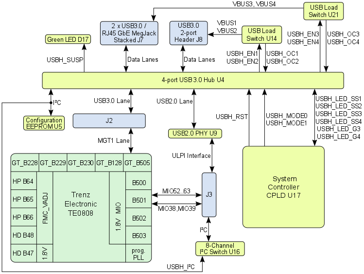
Figure 3: TEBF0808 USB3.0 interface
MPSoC's PS GT Bank 505 Peripheral Interfaces
On the PS GT Bank 505 is beside the USB3.0 Lane also the interface SATA, Display-Port and PCI Express connected.
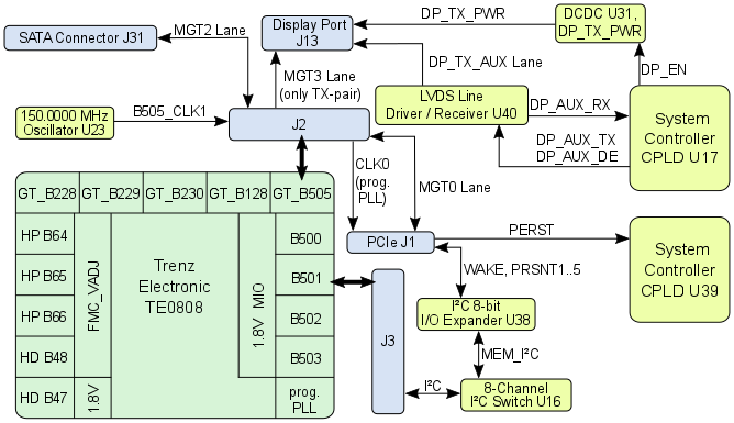
Figure 4: TEBF0808 USB3.0 interface
MGT Interfaces SFP+ and Firefly
Overview
Content Tools