Setup of your own project
The project wizard of Quartus lite guides through the setup of a project.
Before using it, it is suggested to create a project directory for storing it via a file browser.
Quartus lite does not create a folder for you. The generation of the bootloaders requires a
SoC EDS Shell with root privileges on a windows systems. Their file system access
is limited to the C drive. Therefore it is best practice for Windows users to store the project
on the C drive.
In essence, the project setup consists pointing to the project directory, naming the project,
and adding a device to it.
This guide uses the folder Project and the project itself is named HPSexample.
The steps in detail:
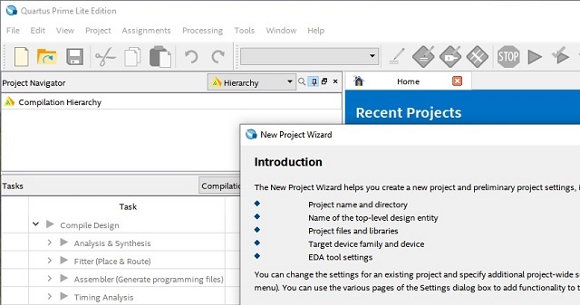
File → New Project Wizard ... Setup the path to the project directory and name the project, click next.
In the following windows - Project Type - and - Add Files - is nothing further required other
than clicking Next.
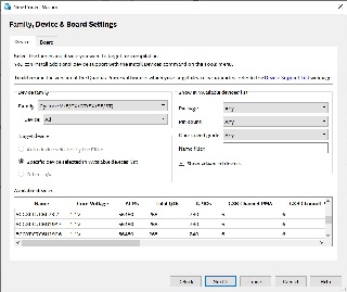
In the next window - Family, Device & Board Settings - it is required to select either a
FPGA Device or a Board from the List.
Copy 5CSEMA5F31C8(N) into the field Name filter , this reduces the Device list, and select it in the list.
In the window EDA Tool Settings just click Next and Finish in the following window - Summary.
Quartus places the folder db, two files HPSexample.qpf and HPSexample.qsf into the project folder
and the setup is accomplished.

Plattform Designer
File → New → Qsys System File
Program - plattform Designer opens
Upper left column - Search field type in hps
Select below: Library - Processors and Peripherals - Hard Processor Systems - Arria V/Cyclone V Hard Processor System
via double click
A new window opens
Tab FPGA Interface:
Uncheck Enable MPU standby and event signals (default)
AXI Bridges
FPGA-to-HPS interface width: unused
HPS-to-FPGA interface width: unused
Lightweight HPS-to-FPGA interface width: unused
Tab Peripheral Pins:
Quad SPI Flash Controller - QSPI pin: HPS I/O Set 0
SD/MMC Controller - SDIO pin: HPS I/O Set 0 - SDIO mode: 4-bit Data
USB Controllers
SPI Controllers
UART Controllers - UART0 pin: HPS I/O Set 0 - UART0 mode: no Flow Control
I2C Controllers - I2C0 pin: HPS I/O Set 1 - I2C1 pin: HPS I/O Set 0
Can Controllers
Tab HPS Clocks:
As is / Accept the default values (for both subtabs)
Tab SDRAM - Subtask Phy Settings:
Memory clock frequency: 333.3 MHz
PLL reference clock frequency: 25 MHz
Tab SDRAM - Subtask - Memory Parameters:
Memory device speed grade: 800.0 MHz
Total interface width: 32
Row Address width: 16
Column Address width: 10
Memory Initialization Options
Memory CAS latency setting: 5
ODT Rtt nominal value: RZQ/6
Memory write CAS latency settings: 5
Tab SDRAM - Subtask - Memory Timing:
tIS (base): 180 ps tIH (base): 140 ps tDS (base) 30 ps tDH (base): 65 ps
tDQSQ: 100 ps tQH 0.38 cycles tDQSCK_ 225 ps
tDQSS: 0.27 cycles tQSH: 0.4 cycles tDSH:0.18 cycles tDSS: 0.18 cycles
tINIT: 500 us tMRD (tMRW): 4 cycles
tRAS: 35.0 ns tRCD: 13.75 ns tRP: 13.75 ns tREFI (tREFIab): 7.8 us tRFC (tRFCab): 350.0 ns tWR: 15.0 ns
tWTR: 4 cycles tFAW: 40 ns tRRD: 12.0 ns tRTP: 12.0 n
Tab SDRAM - Subtask - Board Settings:
Board Skews
Maximum CK delay to DIMM/device: 0.03
Maximum DQA delay to DIMM/device: 0.02
Minimum delay between CK and DQS: 0.09
Maximum delay between CK and DQS: 0.16
Maximum skew within DQS group: 0.01
Maximum skew between DQS groups: 0.08Average delay difference between DQ and DQA: 0.0
Maximum skew within address and command bus: 0.03Average delay difference between address and command and CK: 0.0
Bottom left → Click Finish
To change or correct these parameters later click onto the IP cores top entry in the list in the
Tab System Control - Column Name - hps_0
Add Connections via klicking into the circle MARKED with red rectangle
hps_0 - h2f_reset → clk_0 - clk_in_reset
clk_0 - clk → hps_0 - f2h_sdram0_data
Is this Step NEEDED?!?!?
Hit for good measure:
System → Assign Base Addresses
System → Assign Interrupt Numbers
System → Assign Custom Instruction Opcodes
System → Create Global Reset Network
Bottom right corner → Hit Generate HDL test
A new window opens, forcing to save the design. Give the file a name e.g. PlatformEditorHPS.qsys .
New window opens, under Synthesis, select which Hardware Language you prever Verilog ↔ VHDL
( Check - Create block symbole file (.bsf)
Click Generate and wait → Must be "Save System: completed successfully"
Hit close, Generate HDl window closes
Hit Finish, Plattform Editor window closes
FRAGE: Enable MPU Interrupts auswählen, dann muss das verbunden werden oder Exportiert, wohin / womit?
Notification opens, add file PlattformEditorHPS.qip / .sip (Not Generated, uncheckt simulate)
Add File PlattformEditorHPS.qip into Quartus via Project → Add/Remove Files in Project ...
window Settings - HPSexample opens
Hit Rectangle ... and select path:
C:\temp\Project\PlatformEditorHPS\synthesis click open
In window Settings - HPSexample click OK
In Project Navigator use the Drop-down Menu for changing from Hierarchy to Files and right click onto the
TCL script loßlassen
Tools → TCL Scripts ...
New window - TCL Scripts - opens, select
Project1 → PlatformEditorHPS → synthesis → submodules → hps_sdram_p0_pin_assignments.tcl
Click Run
When finished, new window opens, showing ... click OK
In TCL Scripts window click Close
Hit Processing → Start Compilation
Wait until the compilation has finished , this must finish without any error, warnings and critical warnings are acceptable
Overview
Content Tools