TE0320 is provided with 4 system DIP slide switches as shown in the figure below: S1A, S1B, S1C, S1D.
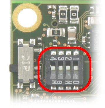
DIP slide switches S1[A:D].
Please note the 4 switch labels are on one side and the <ON> label is on the opposite side.
DIP slide switches S1[A:D] condition the value of some system signals as described in the table below.
switch | S1 label | signal name | <OFF> | <ON> |
|---|---|---|---|---|
S1A | 1 | EEPROM serial data connection to USB FX2 microcontroller | the USB FX2 microcontroller CANNOT read / write the serial EEPROM | the USB FX2 microcontroller can read / write the serial EEPROM |
S1B | 2 | M2 | mode pin M2 = 1 | M2 = 0 |
S1C | 3 | M1 | mode pin M1 = 1 | M1 = 0 |
S1D | 4 | /MR (master reset) | module running | module reset |
S1X settings description.
DIP slide switch S1A (EEPROM serial data connection to USB FX2 microcontroller)
DIP slide switches S1A is ON by default, to allow the USB FX2 microcontroller to read the serial EEPROM and enumerate as a custom/specific USB device.
- When DIP slide switches S1A is ON, the USB FX2 microcontroller can (re)write the (old) serial EEPROM to, for example, store a (new) custom/specific firmware.
- When DIP slide switch is OFF, the USB FX2 microcontroller cannot read the serial EEPROM and enumerates as a Cypress USB generic driver. It is used for boot recovery.
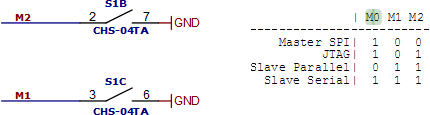
DIP slide switches S1B and S1C (Mode PIN: selection of the way to program SPI Flash)
Mode pins M2 (S1B), M1 (S1C), M0 tell the FPGA how the bitstream will be loaded. See this section for more information.
DIP slide switches S1D (Master Reset of TE0320)
DIP slide switch S1D is OFF by default, to allow the USB FX2 microcontroller and the FPGA to operate regularly.
- When DIP slide switches S1D is ON, the TE0320 is in reset state.
- When DIP slide switch is OFF, the TE0320 operates regularly (regular state).
During the transition from reset state (S1D ON for example) to regular state (S1F OFF), the USB FX2 microcontroller reload the serial EEPROM in RAM and the FPGA reload the bitstream from SPI Flash.
Overview
Content Tools