The (generation 3)TE USB FX2 driver should be already installed and a Generation 3 firmware should be already programmed in USB FX2 microcontroller's EEPROM and RAM.
Insert the TE USB FX2 module with the USB EEPROM enabled (when TE USB FX2 module is powered on).
- A) TE USB FX2 module is seen under Device Driver as a Trenz Electronic Device.
- B) TE USB FX2 module is seen under Device Driver as a DEWESoft Device. In this case, you should start a Recovery boot procedure.
Open a USB Firmware Upgrade Tool (double click OpenFutNet.exe).
- A) TE USB FX2 module is seen under Device Driver as a Trenz Electronic Device.
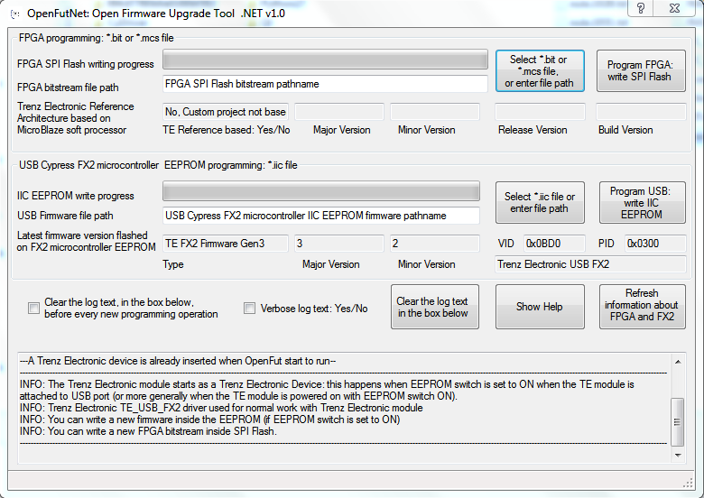
OpenFutNet starts: Trenz Electronic device already inserted
- B) TE USB FX2 module is seen under Device Driver as a DEWESoft Device. You should start a Recovery Boot; you are not able to go any further in FPGA Programming.
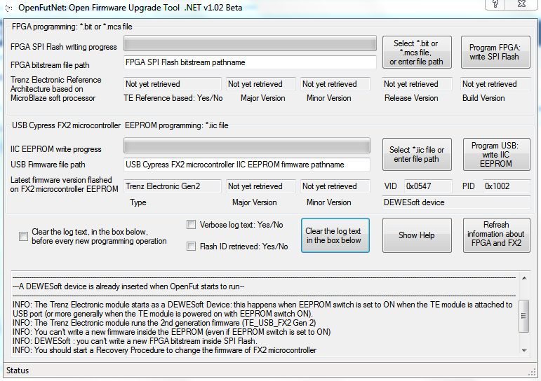
OpenFutNet starts: DEWESoft device already inserted
Press the “Select *.bit or *mcs file, or enter file path” button corresponding to the FPGA bitstream file pathname selection.
Select a suitable *.bit or *.mcs FPGA bitstream file.
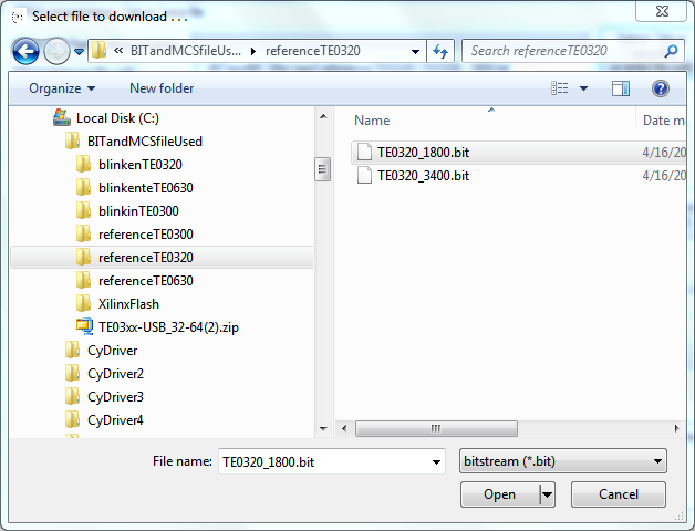
Select the bitstream file to download
Press the “Program FPGA: write SPI Flash” button if you want the *.bit or *.mcs file to be written into the SPI Flash.
The OpenFutNet tool will then attempt to erase the SPI Flash memory.
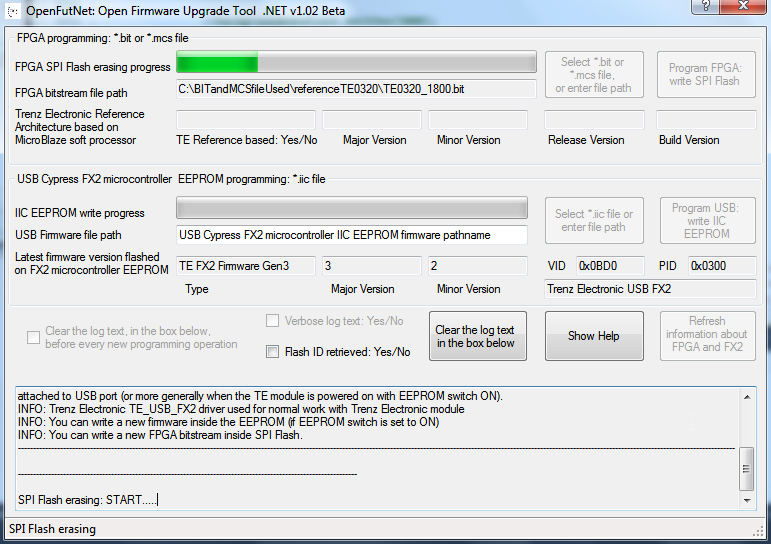
SPI Flash memory erasing
If the SPI Flash memory erasing is successful, the OpenFutNet tool will then attempt to write the SPI Flash memory, if the corresponding box has been selected.
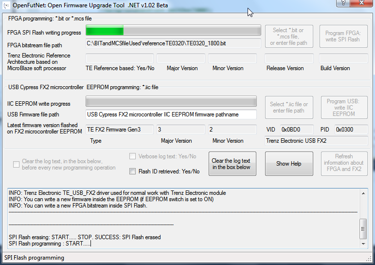
SPI Flash programming
If the SPI Flash memory programming is succesful, FPGA will try to configure from SPI Flash memory. This step take the name of “DONE PIN Checking”. SPI Flash programming can be ended successfully, but the “DONE PIN Checking” can end successfully or with a failure. When the configuration process successfully completes, the FPGA either actively drives the DONE pin High (DriveDone) or allows the DONE pin to float High using either an internal or external pull-up resistor, controlled by the DonePin bitstream generator option.
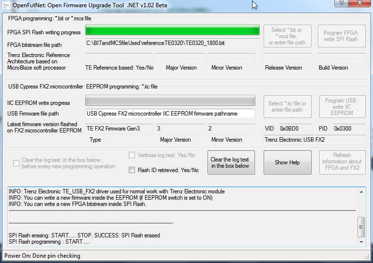
DONE PIN Checking
Two results are possible:
- Status: SUCCESS ("DONE PIN Checking: SUCCESS")
- Status. WARNING ("DONE PIN Checking: FAILURE")
Status: SUCCESS ("DONE PIN Checking: SUCCESS")
If the bitstream (*.bit or *.mcs) of correct FPGA is selected (for example: TE0320 for TE0320 but also Spartan3A 1800 for Spartan3A 1800 FPGA, not Spartan3A 3400 for Spartan3A 1800) and the switches are correctly setted, the “DONE PIN Checking” should end successfully and the FPGA should be ready to work.
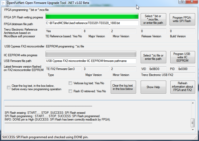
DONE PIN check: Success
Status. WARNING ("DONE PIN Checking: FAILURE")
SPI Flash programming can be ended successfully, but the “DONE PIN Checking” can fails. This may happens if the bitstream of wrong FPGA is selected (TE0300 for TE0320, Spartan3E for Spartan3A FPGA, Spartan3A 3400 for Spartan3A 1800 ) or if the switches are not correctly set.
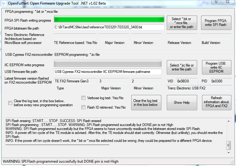
DONE PIN check: failure
In the case of "DONE PIN Checking: SUCCESS" the FPGA Configuration Procedure is ended.
Otherwise ( "DONE PIN Checking: FAILURE") you could try a power off/on cycle (turn the module off and on with the correct switches setting). If this solution doesn't work, you have almost certainly programmed the wrong bitstream in the SPI Flash memory.
Overview
Content Tools