TE USB FX2 module has a flexible IIC (aka I2C) bus on-board as outlined in the figure below.
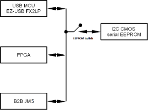
I2C bus topology.
The I2C signals on the TE USB FX2 module are listed and described in the table below
name | definition | description |
|---|---|---|
SDA | serial data | This is a bidirectional pin used to transfer addresses and data into and out of a device. |
SCL | serial clock | This signal is used to synchronize the data transfer to and from a device. |
I2C signals summary.
The I2C bus is typically used by the USB FX2 microcontroller to write USB firmware to the serial EEPROM. In this case,
the I2C port of the FPGA must be set in slave mode (SCL pin as input), the device attached to the I2C port of B2B J(M)5 connector must be set to slave mode.
The USB FX2 microcontroller can operate just in I2C master mode (default operation). If the user wants to set another device attached to the I2C bus as master device, the USB FX2 microcontroller shall three-state (Z = high impedance) its SCL and SDA pins.
If the FPGA is set to I2C master mode, it can write to or read from serial EEPROM (always slave mode) and B2B connector J(M)5 (attached device set to slave mode).
If the device attached to the I2C port of B2B J(M)5 connector is set to master mode, it can write to or read from serial EEPROM (always slave mode) and FPGA I2C port (set to slave mode).
Possible I2C operation modes are summarized in the table below.
core | EZ-USB FX2LP | FPGA | B2B J(M)5 | serial EEPROM |
|---|---|---|---|---|
default | master | slave | slave | slave |
custom | inactive | master | slave | slave |
custom | inactive | slave | master | slave |
I2C bus modes summary.
TE USB FX2 module reference design includes an HDL core managing the fast mode (400 kHz) I2C communication between the Xilinx MicroBlaze embedded soft-processor and the EZ-USB FX2LP USB FX2 microcontroller.
I2C pins on B2B connector J(M)5 cannot be used as GPIOs (general purpose I/Os), as these bus signals are pulled up to 3.3V.
Overview
Content Tools