 |  |  |
|---|
PS Peripherals (on-board)
| Chip/Interface | IC | PS7 Peripheral | |
|---|---|---|---|
| SPI Flash | S25FL127SABMFV10 | QSPI0 | 16 MByte Flash |
| I2C EEPROM | 24xx64 | I2C0 | 8 KByte EEPROM |
| RTC I2C | RV-3029 | I2C0 | |
| RTC Interrupt | RV-3029 | GPIO - MIO0 | |
| User LED | GPIO - MIO7 |
Mapping table for on-board IC to PS7 Peripherals
| MIO Pin | Mapped to | Pull up/down | Notes |
|---|---|---|---|
| 0 | GPIO | Up | RTC Interrupt |
| 1 | QSPI0 | ||
| 2 | QSPI0 | Down | |
| 3 | QSPI0 | Down | |
| 4 | QSPI0 | Down | Override to up on base for bootmode change |
| 5 | QSPI0 | Up | |
| 6 | QSPI0 | Down | |
| 7 | GPIO | Down | On-board LED |
| 8 | CAN1 TXD | Down | CAN transceiver |
| 9 | CAN1 RXD | CAN transceiver | |
| 10 | SPI1 MOSI | ||
| 11 | SPI1 MISO | ||
| 12 | SPI1 SCLK | ||
| 13 | SPI1 SS0 | ||
| 14 | I2C0 SCL | Up | On-board RTC, and EEPROM |
| 15 | I2C0 SDA | Up | On-board RTC, and EEPROM |
Recommended Peripheral mapping for MIO Voltage bank 0.
PS7 UART
There is no fixed mapping for PS7 UART, if needed it can be mapped to free pins from MIO1 Bank or via EMIO to PL pins.
Recommended mapping for primary (console, debug) UART are MIO52, MIO53 for all cases when MIO1 is not used for off-board Gigabit ETH PHY.
PL Peripherals
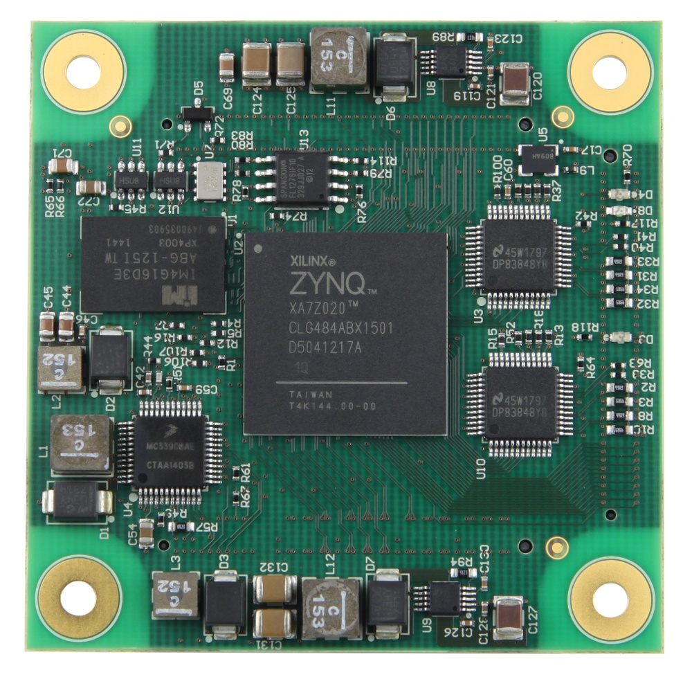
Both Ethernet PHY IC's are connected to PL pins in Bank 34, all PHY IC pins are connected to FPGA pins, there is no sharing of signals for the two PHY's.
PUDC pin is connected with pull-up to 3.3V those pre-configuration pull-ups are disabled by default. Strapping resistor exist to change the PUDC mode.
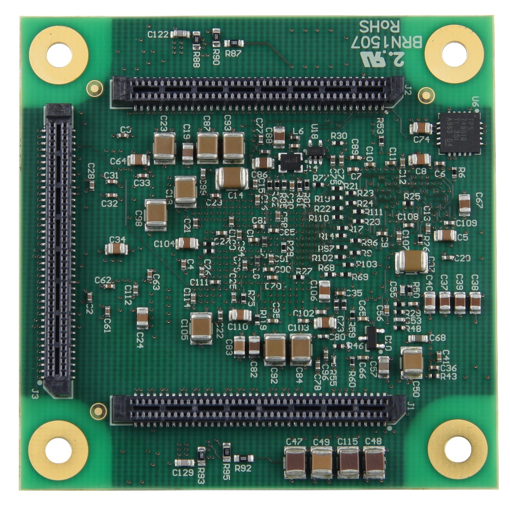
PS and PL Banks
| Bank | VCCIO | B2B I/O Pins | Notes |
|---|---|---|---|
| 500 | 3.3V | 0 | |
| 501 | USER J2.4 B2B | 36 | MIO1 VREF is connected to resistor divider to support HSTL18 |
| 13 | USER J1.39 B2B | 48 | Differential routing |
| 33 | 3.3V | 33 | Single ended routing |
| 34 | 3.3V | 0 | Ethernet PHY's |
| 35 | 3.3V | 42 | Single ended routing |
| 0 | 3.3V | 4 | JTAG, note 3 pins can be used as input only from PL Fabric |
Clock sources
| IC | Description | Frequency | Used as |
|---|---|---|---|
| U14 | MEMS Oscillator | 33.3333 MHz | PS7 PLL clock |
| U5 | MEMS Oscillator | 25 MHz | Ethernet PHY Clock |
| U7 | RTC (internal oscillator) | 32.768 KHz | Used by RTC, CLKOUT of RTC not connected |
LED's
| Designator | Color | Connected to | Active Level | IO Standard |
|---|---|---|---|---|
| D9 | Green | DONE | Low | not applicable |
| D8 | RED | MIO7 | High | not applicable |
| D4 | Green | PL pin V18 | High | LVCMOS33 |
XADC Usage
| XADC Pin | Connected to | Notes |
|---|---|---|
| AD0 | B2B | |
| AD1 | B2B | |
| AD3 | B2B | |
| AD4 | B2B | |
| AD5 | B2B | |
| AD7P | B2B | |
| AD7N | GND | |
| AD8 | B2B | |
| AD9 | B2B | |
| AD10 | B2B | |
| AD12 | B2B | |
| AD13 | B2B | |
| AD14 | B2B | |
| AD15 | B2B |
XADC is used with internal reference option.
Note the XADC capable pins are not routed differentially to the B2B connector. The performance and usability of the XADC must be evaluated.
Ethernet
There are two 100Mbit Extreme Temperature Ethernet PHY's DP83848YB on the board. Datasheet is available from TI, Literature number SNLS208H. Both PHY's are connected with all I/O Pins to FPGA Bank 34 (VCCIO = 3.3V). PHY Clock 25MHz source is provided from MEMS Oscillator. All LED outputs have on-board pull-ups. Outputs to Magnetics have also required termination resistors on board.
Both PHY's must be operated in MII Mode, other modes are not supported. It is possible to use PS ENET0 or ENET1 via EMIO routing or Ethernet IP Cores implemented in PL Fabric.
| ETH1 | ETH2 | Pullup | Notes | |
|---|---|---|---|---|
| CTREF | J3.57 | J3.25 | Magnetics center tap voltage | |
| TD+ | J3.58 | J3.28 | on-board | |
| TD- | J3.56 | J3.26 | on-board | |
| RD+ | J3.52 | J3.22 | on-board | |
| RD- | J3.50 | J3.20 | on-board | |
| LED1 | J3.55 | J3.23 | on-board | |
| LED2 | J3.53 | J3.21 | on-board | |
| LED3 | J3.51 | J3.19 | on-board | |
| POWERDOWN/INT | L21 | R20 | on-chip | It is recommended to configure FPGA I/O as input with Pullup or as output driving 1 if Interrupt not used. |
| RESET_N | M15 | R16 | on-chip | It is recommended to configure FPGA I/O as input with Pullup or as output (active low PHY Reset). |
It is recommended to add IOB TRUE constraint for the MII Interface pins.
When connecting the PHY's to Zynq PS ETH0, ETH1 EMIO GMII Interfaces it is recommended to use GMII to MII Wrap IP Core. This IP core maps the EMIO GMII to external MII Interface.
Legal Notices
Unable to render {include} The included page could not be found.
Document Change History
| Date | Revision | Authors | Description |
|---|---|---|---|
| 2015-05-10 | Work in progress | ||
All |
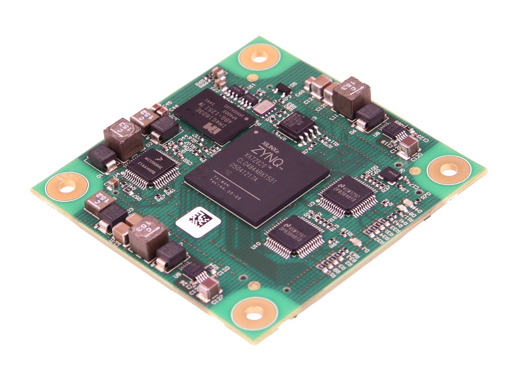
Overview
Content Tools