Table of Contents
Overview
The Trenz Electronic TE0703 is...
Block Diagram
Main Components
Key Features
Initial Delivery State
Interfaces and Pins
Board to Board (B2B) I/O's
For detailed information about the pin out, please refer to the Master Pinout Table.
Ethernet
USB Interface
JTAG Interface
JTAG access to the Xilinx is provided through B2B connector JM2.
JTAG Signal | B2B Connector Pin |
|---|---|
| TCK | JM2-99 |
| TDI | JM2-95 |
| TDO | JM2-97 |
| TMS | JM2-93 |
JTAGEN pin in B2B connector JM1 should be kept low or grounded for normal operation.
System Controller I/O Pins
Special purpose pins are connected to smaller System Controller CPLD and have following default configuration:
| Pin Name | Mode | Function | Default Configuration |
|---|---|---|---|
| EN1 | Input | Power Enable | No hard wired function on PCB, when forced low pulls POR_B low to emulate power on reset. |
| PGOOD | Output | Power Good | Active high when all on-module power supplies are working properly. |
| NOSEQ | - | - | No function. |
| RESIN | Input | Reset | Active low reset, gated to POR_B. |
| JTAGEN | Input | JTAG Select | Low for normal operation. |
Boot Mode Pin
By default the TE-0715 supports QSPI and SD Card boot modes which is controlled by the MODE input signal from the B2B connector.
MODE Signal State | Boot Mode |
|---|---|
high or open | SD Card |
low or ground | QSPI |
LED's
| LED | Color | Connected to | Description and Notes |
|---|---|---|---|
D2 | Green | DONE | Reflects inverted DONE signal, ON when FPGA is not configured, OFF as soon as PL is configured. This LED will not operate if the SC can not power on the 3.3V output rail that also powers the 3.3V circuitry on the module. |
D3 | Red | SC | System main status LED. |
D4 | Green | MIO7 | User controlled, default OFF (when PS7 has not been booted). |
Power
Power Supply
Power supply with minimum current capability of 3A for system startup is recommended.
Power Consumption
| Power Input Pin | Max Current |
|---|---|
| VIN | TBD* |
* TBD - To Be Determined soon with reference design setup.
Technical Specifications
Absolute Maximum Ratings
Assembly variants for higher storage temperature range are available on request.
Please check Lattice datasheet .... for complete list of absolute maximum and recommended operating ratings.
Recommended Operating Conditions
Physical Dimensions
Board size: mm × mm. Please download the assembly diagram for exact numbers
Mating height with standard connectors: 8mm
PCB thickness: 1.6mm
Highest part on PCB: approx. 2.5mm. Please download the step model for exact numbers
All dimensions are given in mm.
Operating Temperature Ranges
Commercial grade: 0°C to +70°C.
Industrial grade: -40°C to +85°C.
Board operating temperature range depends also on customer design- and cooling solution. Please contact us for options.
Weight
.. g - Plain board
.. g - Set of bolts and nuts
Document Change History
Date | Rrevision | Contributors | Description |
|---|---|---|---|
| 2016-06-28 | New overall document layout with shorter table of contents. Revision 01 PCB pictures replaced with the revision 03 ones. Fixed link to Master Pinout Table. New default MIO mapping table design. Revised Power-on section. Added links to related Xilinx online documents. Physical dimensions pictures revised. Revision number picture with explanation added. | ||
| 2016-04-27 | V33 | Philipp Bernhardt, Antti Lukats, Thorsten Trenz, Emmanuel Vassilakis | Added the table "Recommended Operating Conditions" Storage Temperature edited. |
| 2016-03-31 | V10 | Philipp Bernhardt, Antti Lukats, Thorsten Trenz | Initial version. |
Hardware Revision History
| Date | Revision | Notes | PCN |
|---|---|---|---|
| - | 01 | Prototypes | |
| - | 02 | ||
| - | 03 | ||
| - | 04 | ||
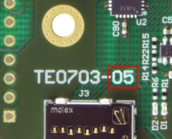
| 10.08.2016 | 05 |
Hardware revision number is printed on the PCB board together with the module model number separated by the dash.
Disclaimer
Unable to render {include} The included page could not be found.
Overview
Content Tools