Additional Master Pinout Viewer/XDC-Generator is available on Trenz Electronic Download - Pinout
How to Use This Guide
- This guide is split into two tables:
- Module Power Connection Table shows the power source of the different FPGA banks and components of the different module boards.
Carrier Board Power Connection Table shows the power source of the B2B connectors with pins, schematic names and available options of the different carrier boards.
- The PCBs have fixed and variable user supplied I/O voltage pins. Variable power supply pins are colored in four groups (VCCIOA, VCCIOB, VCCIOC and VCCIOD).
- Find your module model on the Module Power Connection Table and check the power supply of the different FPGA banks.
- If the power supply is variable(colored), go to the Carrier Board Power Connection Table and see how it's connected on your carrier board. Often the power source can be selected by jumper, resistor or variable used from other connector pin of the carrier board. So use the schematic name or the component designator from the table to search for the available options in the PCB schematics or TRM.
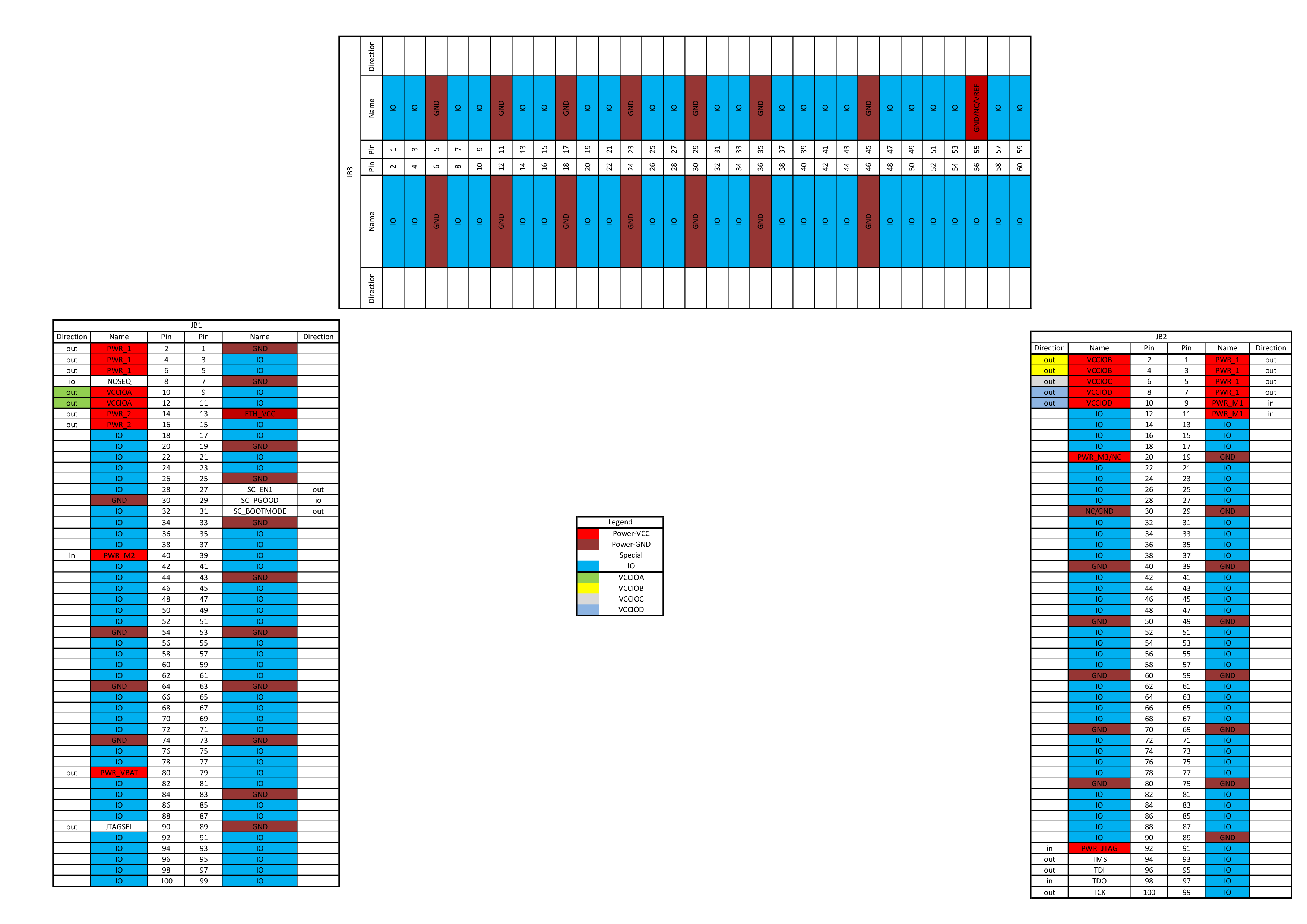
Module Power Connection Table
| Group | 1 | 2 | 3 | 4 | 5 | 6 | 7 | 8 | |||||||||||||||||||||
|---|---|---|---|---|---|---|---|---|---|---|---|---|---|---|---|---|---|---|---|---|---|---|---|---|---|---|---|---|---|
| Module Model | Bank | IOs | Type | Voltage | Bank | IOs | Type | Voltage | Bank | IOs | Type | Voltage | Bank | IOs | Type | Voltage | Bank | IOs | Type | Voltage | Bank | IOs | Type | Voltage | Bank | IOs | Type | Voltage | |
| TE0710 | B15 | 48 | HR | VCCIOA | - | - | - | - | - | - | - | - | B34 | 50 | HR | VCCIOD | B16 | 6 | HR | 3.3V | B14 | 8 | HR | 3.3V | 2x 100Mbit ETH | ||||
| TE0711 | B15 | 48 | HR | VCCIOA | B34 | 36 | HR | VCCIOB | B14 | 18 | HR | 3.3V | B35 | 50 | HR | VCCIOD | B16 | 6 | HR | 1.8V | B14 | 8 | HR | 3.3V | B34 | 8 | HR | VCCIOB | |
| TE0712 | B16 | 48 | HR | VCCIOA | B13 | 20 | HR | VCCIOB | B14 | 18 | HR | 3.3V | B15 | 50 | HR | VCCIOD | B13 | 6 | HR | VCCIOB | B14 | 8 | HR | 3.3V | 1x 100Mbit ETH / B13 | 4 | HR | VCCIOB | |
| TE0715-xx-15 | B13 | 48 | HR | VCCIOA | B34 | 16 | HR | VCCIOC | B34 | 18 | HR | VCCIOC | B35 | 40 | HR | VCCIOD | B501 | 6 | MIO | 1.8V | B500 | 8 | MIO | 3.3V | 1x Gbit ETH | SGMII | |||
| TE0715-xx-30 | B13 | 48 | HR | VCCIOA | B34 | 16 | HP | VCCIOC | B34 | 18 | HP | VCCIOC | B35 | 40 | HP | VCCIOD | B501 | 6 | MIO | 1.8V | B500 | 8 | MIO | 3.3V | 1x Gbit ETH | SGMII | |||
| TE0720 | B35 | 48 | HR | VCCIOA | B34 | 36 | HR | VCCIOB | B33 | 18 | HR | VCCIOC | B13 | 50 | HR | VCCIOD | B501 | 6 | MIO | 1.8V | B500 | 8 | MIO | 3.3V | 1x Gbit ETH | SGMII | |||
| TE0820* | B25 B26 | 48 | HD | VCCIOA | B64 | 50 | HR | VCCIOD | 6 | MIO | 1.8V | 8 | MIO | 3.3V | 1x Gbit ETH | ||||||||||||||
| TE0741 | B13 | 48 | HR | VCCIOA | B16 | 16 | HR | VCCIOB | B15 | 18 | HR | VCCIOC | B12 | 50 | HR | VCCIOD | GTX | 1 Lane | B14 | 8 | HR | 3.3V | GTX | 2 Lanes | GTX | ||||
| TE0742* | |||||||||||||||||||||||||||||
| TE0841 | B64 | 48 | HR | VCCIOA | B66 | 18 | HP | VCCIOB | B68 | 18 | HP | VCCIOC | B67 | 50 | HP | VCCIOD | GTH | 1 Lane | B65 | 8 | HR | 3.3V | GTH | 2 Lanes | GTH | ||||
| TE0842* | |||||||||||||||||||||||||||||
I/O resource comparison for all 4x5 modules. There are maximum 4 user supplied I/O voltages (VCCIOA, VCCIOB, VCCIOC and VCCIOD).
Attention: Maximum supply voltage for HP banks is 1.8V.
Module B2B FPGA-Banks and Voltages
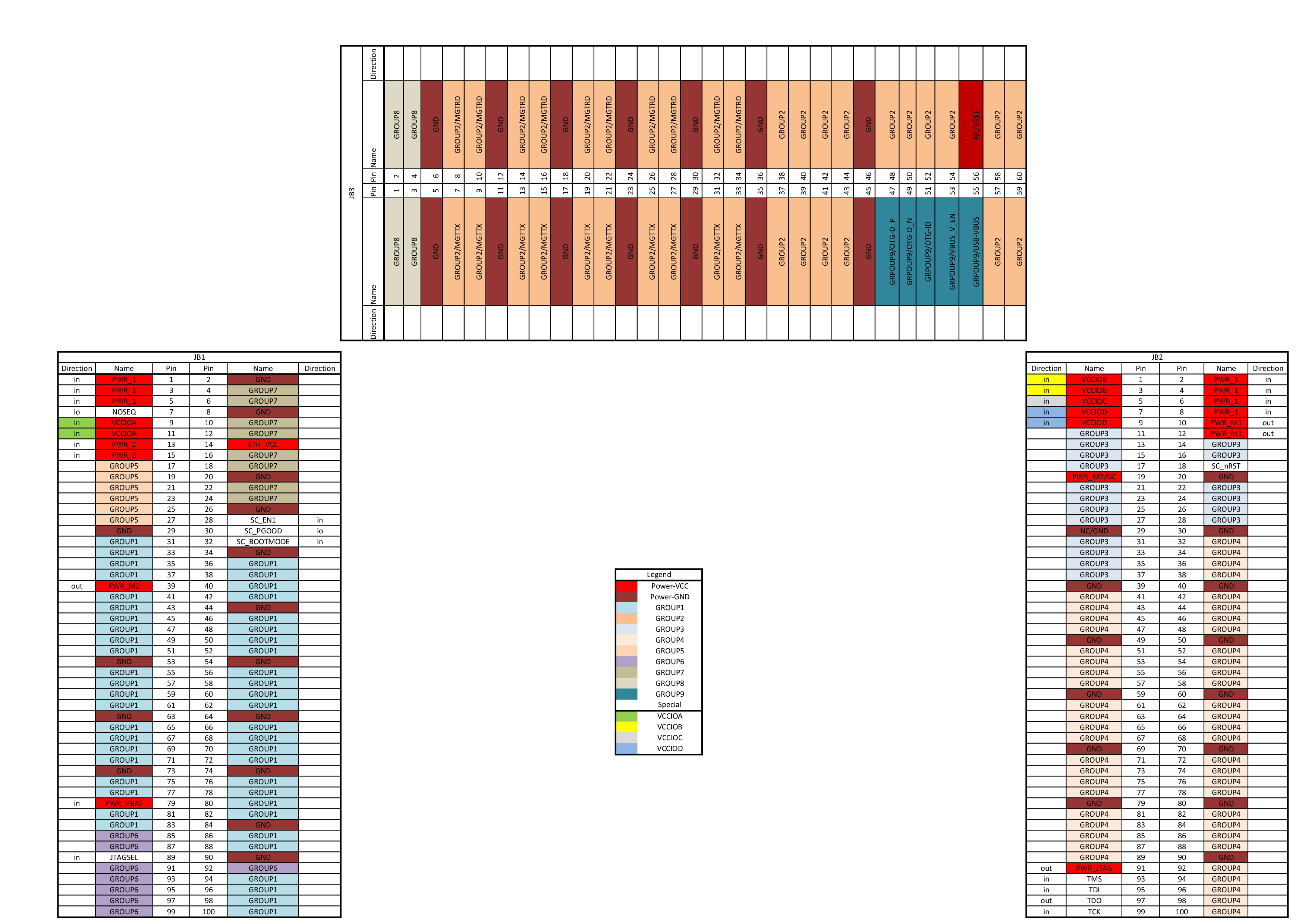
Attention: Currently not complete, verify with Schematics
Module basic power pin assignment (Top View)
Carrier Board Power Connection Table
| IO Voltage | B2B Connector | Carrier Boards | |||||||||||
|---|---|---|---|---|---|---|---|---|---|---|---|---|---|
| Name | Direction* | JB1 | JB2 | TE0701 | TE0703 Rev 01 - Rev 04 | TE0703 Rev 05 | TE0705 | TE0706 | |||||
| Pin | Pin | Schematic Name | Value,Option,Comp. | Schematic Name | Value,Option,Comp. | Schematic Name | Value,Option,Comp. | Schematic Name | Value,Option,Comp. | Schematic Name | Value,Option,Comp. | ||
| PWR_1 | out | 2,4,6 | 1,3,5,7 | 5V0 | 5V | 3.3V | 3.3V | 3.3V | 3.3V | 5V0 | 5V | 3.3V | 3.3V |
| VCCIOA | out | 10,12 | VIOTB | FMC_VADJ 2V5 3.3VOUT | VCCIO35 | R23→M3.3VOUT J1B-B1 | VCCIOA | J5→M3.3VOUT, M1.8VOUT R23→M3.3VOUT J1-B1 | VIOTB | FMC_VADJ 2V5 3.3VOUT | VCCIO35 | R20->M3.3VOUT/J6B-B32 | |
| VCCIOD | out | 8,10 | VIOTB | FMC_VADJ 2V5 3.3VOUT | VCCIO13 | R26→M3.3VOUT J2B-B1 | VCCIOD | J10→M3.3VOUT, M1.8VOUT R26→M3.3VOUT J2B-B1 | VIOTB | FMC_VADJ 2V5 3.3VOUT | VCCIO13 | R22->M3.3VOUT/J6B-B1 | |
| PWR_2 | out | 14,16 | 3V3IN | 3.3V | 3.3V | 3.3V | 3.3V | 3.3V | 3V3IN | 3.3V | 3.3V | 3.3V | |
| VCCIOB | out | 2,4 | no name | FMC_VADJ 2V5 3.3VOUT | VCCIO34 | J5→M3.3VOUT J1B-B32 | VCCIOB | J8→M3.3VOUT,M1.8VOUT J2B-B32 | VIOTB | FMC_VADJ 2V5 3.3VOUT | 1.8V | 1.8V | |
| VCCIOC | out | 6 | no name | FMC_VADJ 2V5 3.3VOUT | VCCIO33 | R25→M3.3VOUT J2B-B32 | VCCIOC | J9→M3.3VOUT, M1.8VOUT R25→M3.3VOUT J2B-B32 | VIOTB | FMC_VADJ 2V5 3.3VOUT | VCCIO33 | R21->M3.3VOUT | |
| PWR_M1 | in | 9,11 | 3.3VOUT | 3.3V | 3.3VOUT | 3.3V | M3.3VOUT | 3.3V | 3.3VOUT | 3.3V | M3.3VOUT | 3.3V | |
| PWR_M2 | in | 40 | VIOB | 1.8V | M1.8VOUT | 1.8V | M1.8VOUT | 1.8V | VIOB | 1.8V | M1.8VOUT | 1.8V | |
| PWR_M3 | in | 20 | NC | NC | NC | NC | NC | ||||||
| PWR_VBAT | out | 80 | VBAT | B1 | VBAT | J7 | VBAT | J7 | NC | VBAT | J9 | ||
PWR_JTAG | in | 92 | VCCJTAG | VCCJTAG | VCCJTAG | VCCJTAG | VCCJTAG | ||||||
Power comparison of all 4x5 carrier boards. *Power direction based on carrier boards view.There are 4 variable user supplied I/O voltages (VCCIOA, VCCIOB, VCCIOC and VCCIOD). PWR_1 and PWR_2 are fixed from carrier boards. PWR_M1 and PWR_M2 normally use default value from module. NC=Not Connected
Attention: On some carrier boards the user supplied I/O voltages are connected together (red colored schematic names).
Power Pin Connection on different Carrierboards
Attention: Currently not complete, verify with Schematics
Carrierboard basic power pin assignment (Top View)
Overview
Content Tools