Overview
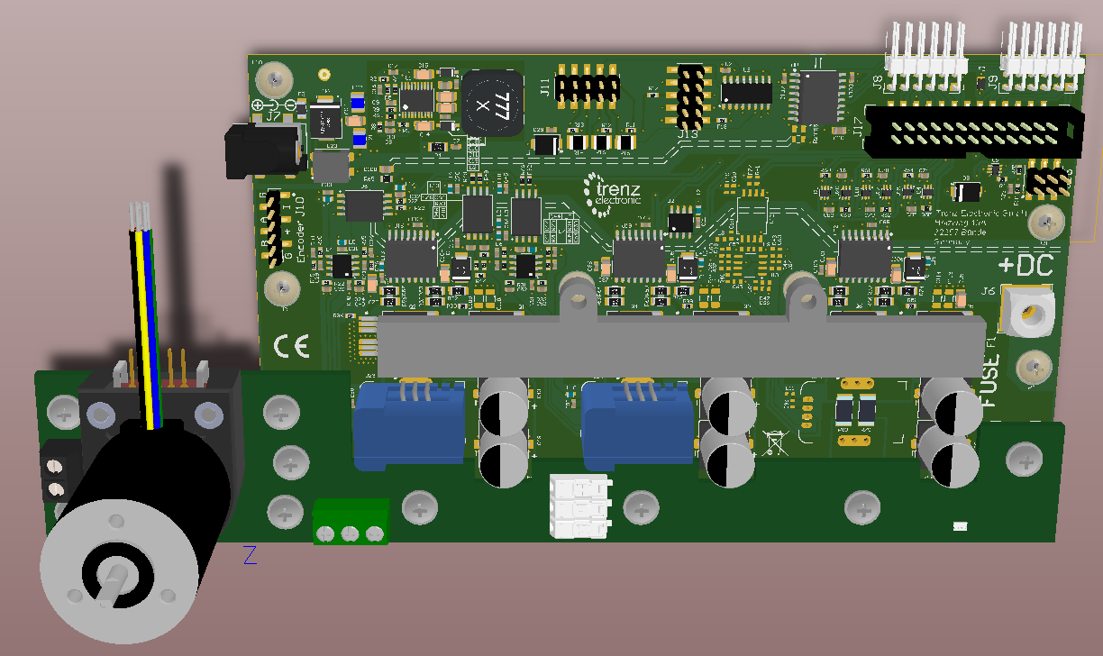
Option 1: with DC +12V Reference Motor Board (Delivery condition)
Option 2: Customer Motor at individual DC +5..48V
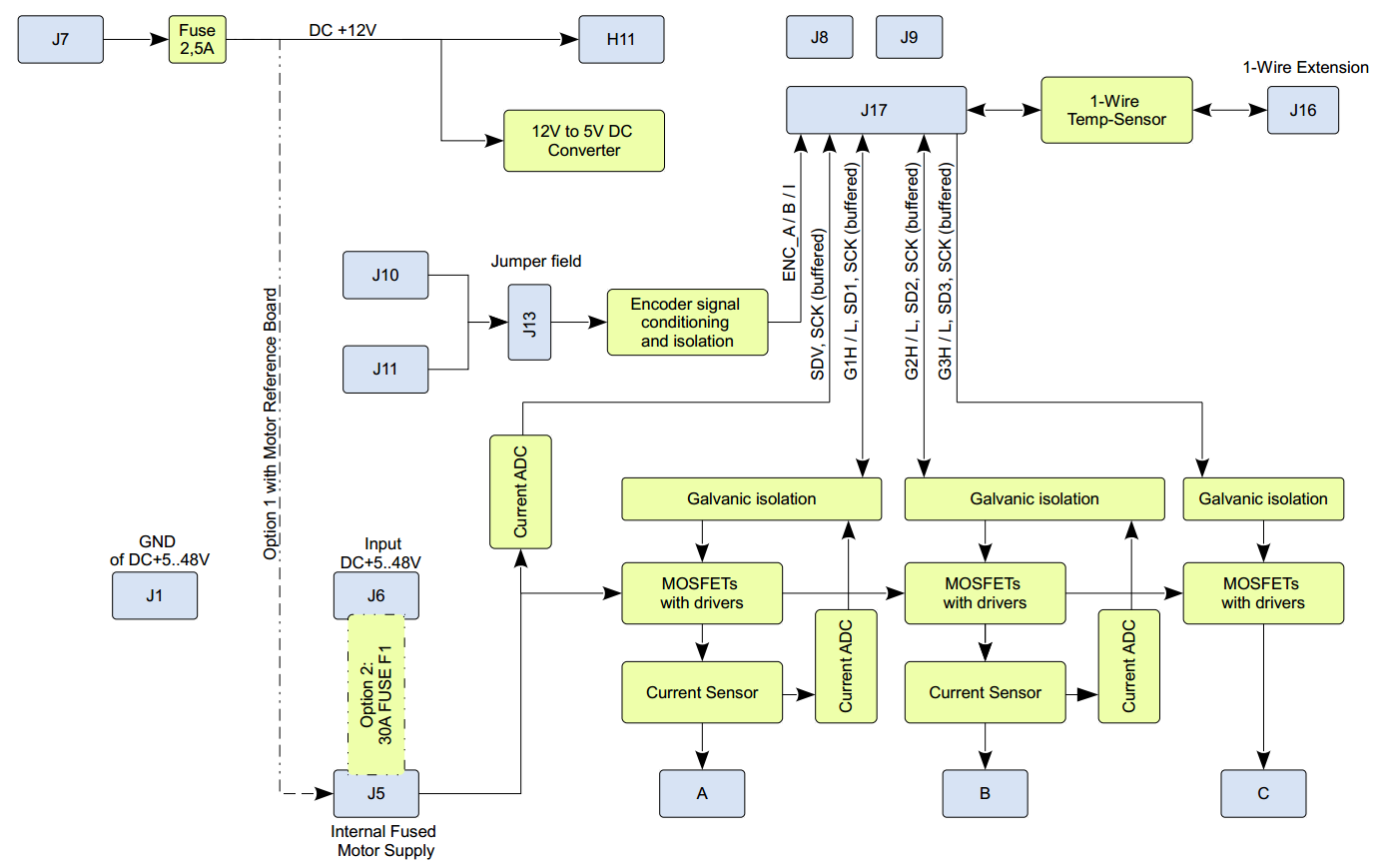
Block Diagram
Main Components
Key Features
Initial Delivery State
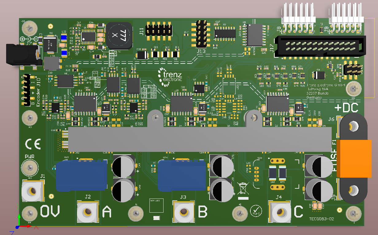
Signals, Interfaces and Pins
Controller Board Connections (Arty etc.)
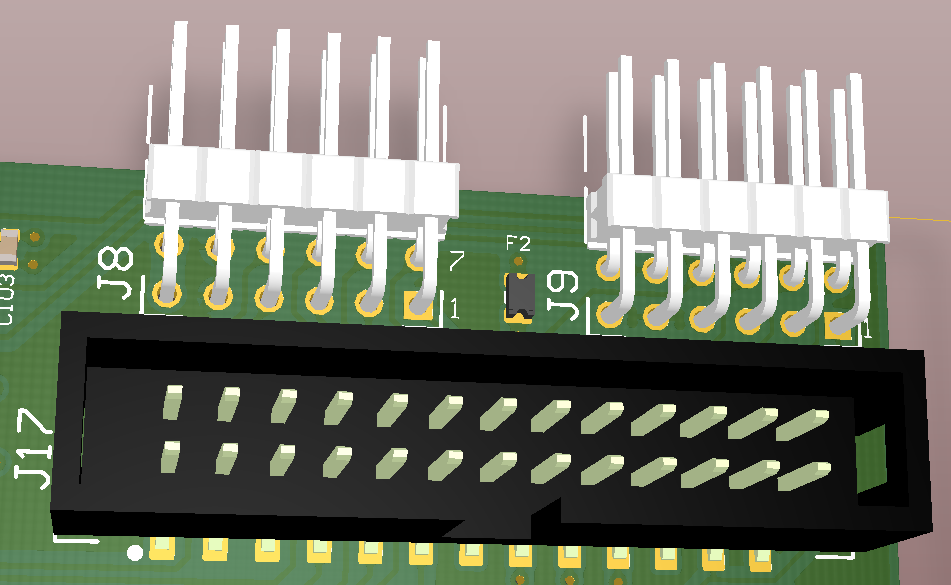
| Signalnames | Connector J8 | Connector J9 | Connector J17 |
|---|---|---|---|
Digital Supply to EDPS | Pin 6, 12: +3.3V | Pin 6, 12: +3.3V Pin 5, 11: GND | Pin 5, 6, 21, 22: +3.3V Pin 1, 2, 25, 26: GND |
Motor Driver PWM Signals to EDPS High and Low Side control signals
| Pin 1: G1H - Ch.A HighSide | Pin 11: G1H - Ch.A HighSide | |
| ADC Clock Signal to EDPS | Pin 1: SCLK | Pin 23: SCLK | |
| Encoder Digital Signals from EDPS | Pin 8: ENC_A | Pin 20: ENC_A | |
| Motor Current ADC "raw" Signals from EDPS (usabel with FPGA IP) | Pin 2: SDI1 - Current Ch.A | Pin 19: SDI1 - Current Ch.A | |
| Supply Voltage ADC "raw" Signal from EDPS (usabel with FPGA IP) | Pin 7: SDIV - from DC_LINK | Pin 24: SDIV - from DC_LINK | |
| 1-Wire bus for temperature measurement | Pin 10: EXT1 - 1-Wire Bus 1 Pin 4: EXT2 - 1-Wire Bus 2 | Pin 4: EXT1 - 1-Wire Bus 1 | |
| Not connected pins | none | none | Pin 13, 14 |
Motor and Power Concept
There are two options available for the motor and power concept:
| Detail | Option 1: Reference Motor Board with DC +12V Supply | Option 2: Customer Motor at individual DC +5..48V | Comment |
|---|---|---|---|
| Motor Supply | From DC +12V Input J7 via Fuse F3 (TODO ... A) | From customer DC Supply to J6 via F1 on Eval Boad | |
| Motor Connection | Motor wires connected to cage clamps on Motor Reference Board J5 (A), J4 (B), J3 (C) | Motor wires connected to bolt screw terminals on Eval Board J2 (A), J3 (B), J4 (C) | |
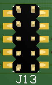
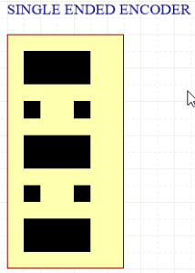
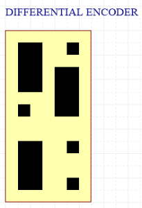
| Encoder Connection | From encoder pins via ribbon cable to Eval Board J10, 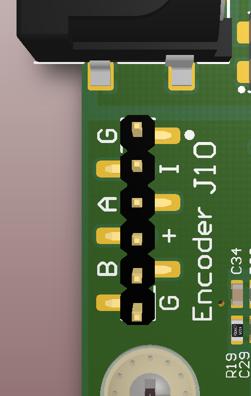 J11 single ended: | From motor to Eval Board J10 (only single ende signals) see left colomn, or to J11 (single OR differential signals): 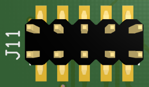 J11 single ended: J11 differential with 100R terminated: | Jumper Settings for encoder signals.
|
Reference Motor Board TEC0060
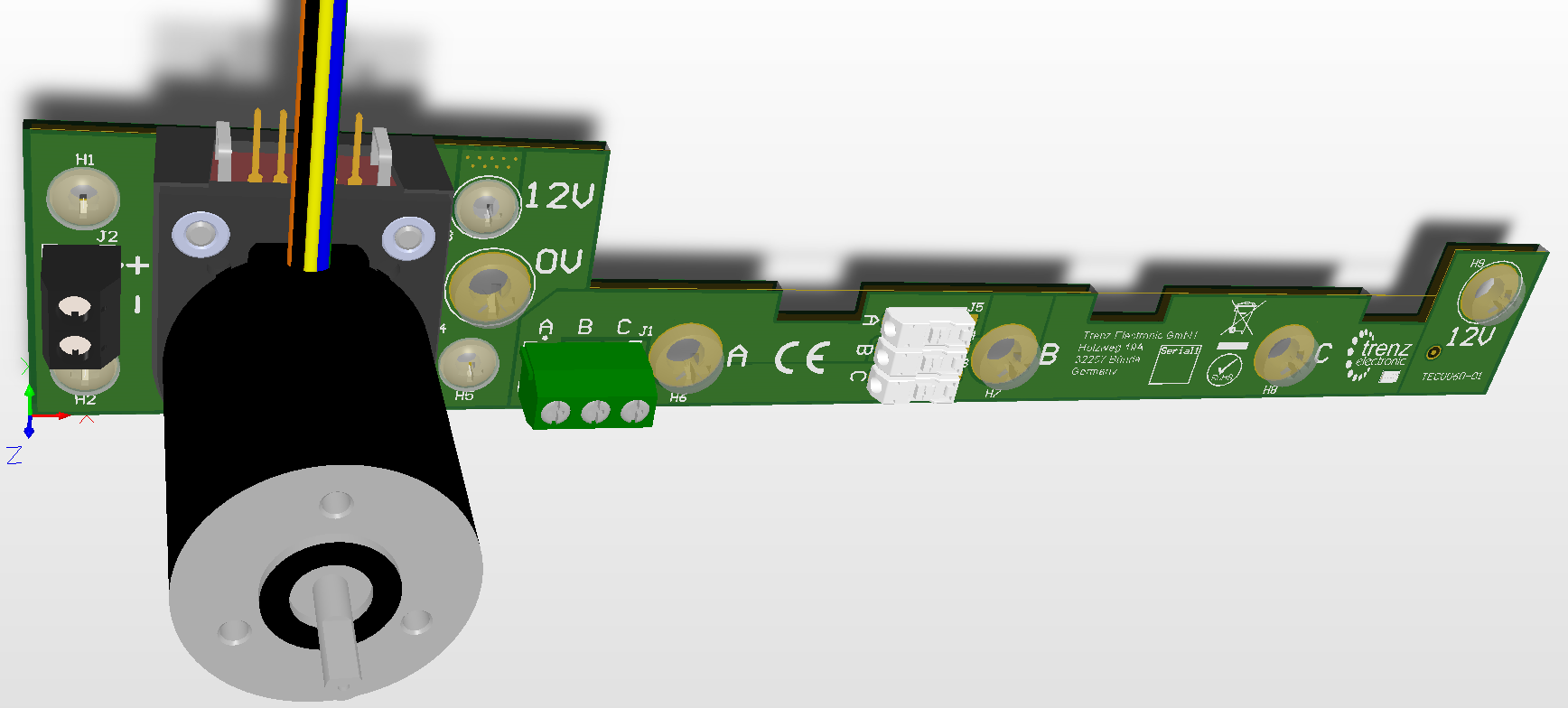
Reference Motor
The manufaturer of the reference motor is Anaheim Automation and the order no. of the delivered combination of the motor with encoder is BLWR111D-24V-10000-1000SI.
The nominal motor voltage is DC 24V whichi is supplied by DC 12V on the Reference Motor Board. This will cause a certain derating in performace.
The datasheet of the motor:
http://www.anaheimautomation.com/manuals/brushless/L010234%20-%20BLWR11%20Series%20Product%20Sheet.pdf
The datasheet of the encoder:
http://www.anaheimautomation.com/manuals/accessories/L010390%20-%20Single%20Ended%20Encoder%20with%20Index%20Channel.pdf
Internal
Temperature Sensor
Onboard a Maxim 1-Wire Temperature sensor DS18S20Z+ is available, which is located on the potential of the FPGA board as close as possible to the central motor MOSFETs.
Addional 1-Wire temperature sensor can be connected by wire to connector J16:
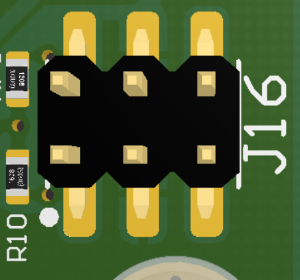
- Pin 1(DQ), 3 (GND),5 (+3.3V) at the same 1-wire bus as the onboard one
- Pin 2(DQ), 4 (GND),6 (+3.3V) at a separate 1-wire bus
Power and Power-On Sequence
Power Supply
+ DC 12V Motor Driver and Motor Supply
The motor drivers and the reference motor on the pre-mounted motor board TEC0060 are supplied by this voltage.
The internal +5V digital supply ist generated out of this +12V supply.
+ DC 5...48V Optional Motor Supply
SAFETY INSTRUCTIONS:
This option is
- only usable at your own risk
- only allowed to be used for electrical specialist for the used electical voltage and power conditions
- only allowed to be used under electrical laboritory conditions
- only allowed to be used in horizontal position on a non conducting surface
- only allowed to be used, if the "Eval Boad high current signals" conducting up to 30A nominal, are covered by isolating, mechanically stable material
The "Eval Boad high current signals" are the motor outputs A, B, C and Fuse F1 Connectors J5 an J6 and further internal connections shown white marked in the following picture:
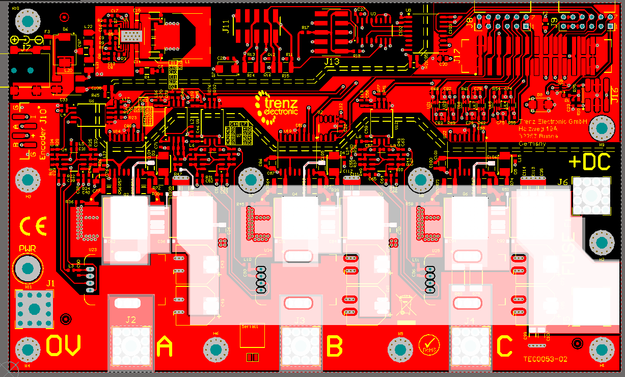
- Highly recommended is to use the delivered "Isolating cover PCB" (marked in green), which needs to be mounted to the mounting holes H1, H9, H3, H4 with the deliverd 10mm isolating spacers:
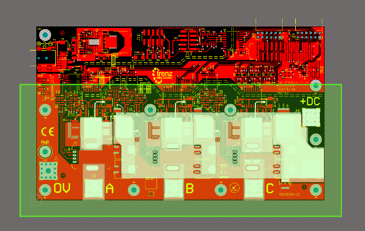
- The used cable lugs need to be isolated in the area outstanding the outer border of the Eval Board.
Intention is to make sure that the "Isolating Cover PCB" is overlapping the conducting material by a minimum of 2 cm.
Initial operation
The option 2 motor supply is only usable after the following steps are done:
- Disconnecting the reference motor board TEC0060 by unmounting its screws and the encoder cable from J10
- Mounting the deliverd 30A Fuse to the connectors J5 and J6 with the deliverd M5 screws
- Connecting with a cable lugs the +DC 5..48V to J6 and the corresponding GND to J1.
- The cable length is limited to 3m.
- Connection the three motor phases to J2 (A), J3 (B) and J4 (C).
- The cable length is limited to 3m.
- Optional: connect the encoder wires to J10 or J11
and set jumper field according to signal specification: differential or single ended
See section TODO for details
Power Consumption
Test Condition:
| VIN Current mA | Notes |
|---|---|---|
| TEC0053-03 +3V3 | TODO mA | |
| TEC0053-03 +12V | TODO mA |
Power-On Sequence
Any power sequence of the three supply sources is allowed:
- +3V3 Supply from the FPGA Board, generated by FPGA Board supply
- +12V and
- optional +5..48V Motor Supply
Variants Currently In Production
TODO:
Technical Specifications
Absolute Maximum Ratings
| Parameter | Min | Max | Units | Notes | Reference document |
|---|---|---|---|---|---|
DC +12V supply | TODO | TODO | V | ||
| DC +5..48V supply | 5 | 48 | V | ||
| DC +3V3 supply | TODO | TODO | V | ||
| PWM Input Logic High Level | TODO | TODO | V | ||
| PWM Input Logic Low Level | TODO | TODO | V | ||
| ADC Digital Output Logic High Level | TODO | TODO | V | ||
| ADC Digital Output Logic Low Level | TODO | TODO | V | ||
| Encoder Input Logic High Level (Differential) | TODO | TODO | V | ||
| Encoder Input Logic Low Level (Differential) | TODO | TODO | V | ||
| Encoder Input Logic High Level (Sigle Ended) | TODO | TODO | V | ||
| Encoder Input Logic Low Level (Sigle Ended) | TODO | TODO | V |
Recommended Operating Conditions
| Parameter | Min | Max | Units | Notes | Reference document |
|---|---|---|---|---|---|
DC +12V supply | 11.5 | 12.5 | V | ||
| DC +5..48V supply | 5 | 48 | V | ||
| DC +3V3 supply | TODO | TODO | V | ||
| PWM Input Logic High Level | TODO | TODO | V | ||
| PWM Input Logic Low Level | TODO | TODO | V | ||
| ADC Digital Output Logic High Level | TODO | TODO | V | ||
| ADC Digital Output Logic Low Level | TODO | TODO | V | ||
| Encoder Input Logic High Level (Differential) | TODO | TODO | V | ||
| Encoder Input Logic Low Level (Differential) | TODO | TODO | V | ||
| Encoder Input Logic High Level (Sigle Ended) | TODO | TODO | V | ||
| Encoder Input Logic Low Level (Sigle Ended) | TODO | TODO | V |
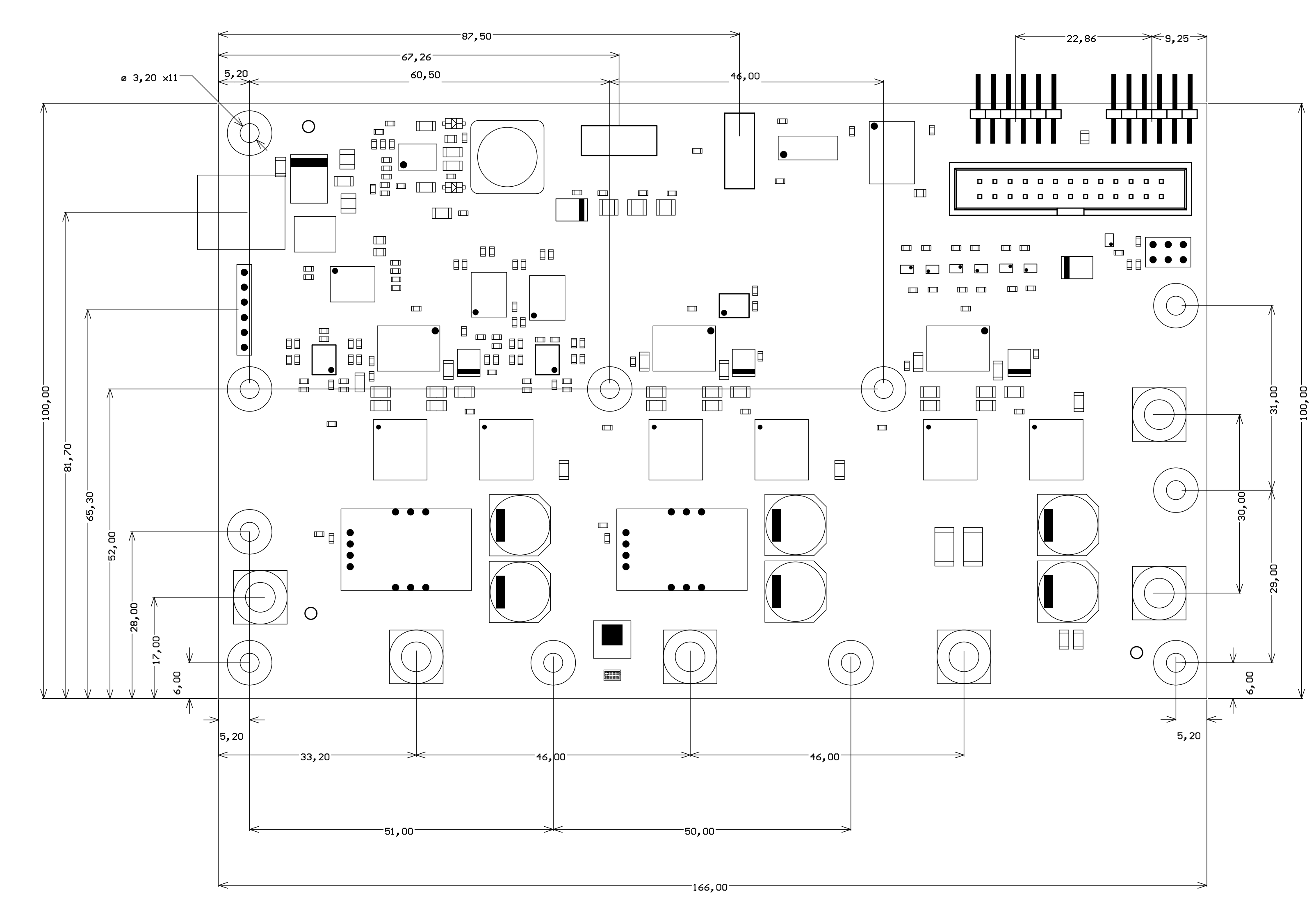
Physical Dimensions
Board size: 100 mm × 166 mm. Please download the assembly diagram for exact numbers.
PCB thickness: 1.75 mm +/-10%
Highest part on PCB: approximately 17 mm. Please download the step model for exact numbers.
All dimensions are shown in mm. Additional sketches, drawings and schematics can be found TODO: here.
Operating Temperature Ranges
Weight
| Variant | Weight in g | Note |
|---|---|---|
| - | TODO |
|
Revision History
Hardware Revision History
| Date | Revision | Notes | PCN Link | Documentation Link |
|---|---|---|---|---|
| 2016-03-27 | 02 | TEC0053-02 |
Hardware revision number is printed on the PCB board in the down right corner.
Document Change History
Date | Revision | Authors | Description |
|---|---|---|---|
| 2017-03-30 |
| Andreas Heidemann | Initial Version |
Disclaimer
Document Warranty
The material contained in this document is provided “as is” and is subject to being changed at any time without notice. Trenz Electronic does not warrant the accuracy and completeness of the materials in this document. Further, to the maximum extent permitted by applicable law, Trenz Electronic disclaims all warranties, either express or implied, with regard to this document and any information contained herein, including but not limited to the implied warranties of merchantability, fitness for a particular purpose or non infringement of intellectual property. Trenz Electronic shall not be liable for errors or for incidental or consequential damages in connection with the furnishing, use, or performance of this document or of any information contained herein.
Limitation of Liability
In no event will Trenz Electronic, its suppliers, or other third parties mentioned in this document be liable for any damages whatsoever (including, without limitation, those resulting from lost profits, lost data or business interruption) arising out of the use, inability to use, or the results of use of this document, any documents linked to this document, or the materials or information contained at any or all such documents. If your use of the materials or information from this document results in the need for servicing, repair or correction of equipment or data, you assume all costs thereof.
Copyright Notice
No part of this manual may be reproduced in any form or by any means (including electronic storage and retrieval or translation into a foreign language) without prior agreement and written consent from Trenz Electronic.
Technology Licenses
The hardware / firmware / software described in this document are furnished under a license and may be used /modified / copied only in accordance with the terms of such license.
Environmental Protection
To confront directly with the responsibility toward the environment, the global community and eventually also oneself. Such a resolution should be integral part not only of everybody's life. Also enterprises shall be conscious of their social responsibility and contribute to the preservation of our common living space. That is why Trenz Electronic invests in the protection of our Environment.
REACH, RoHS and WEEE
REACH
Trenz Electronic is a manufacturer and a distributor of electronic products. It is therefore a so called downstream user in the sense of REACH. The products we supply to you are solely non-chemical products (goods). Moreover and under normal and reasonably foreseeable circumstances of application, the goods supplied to you shall not release any substance. For that, Trenz Electronic is obliged to neither register nor to provide safety data sheet. According to present knowledge and to best of our knowledge, no SVHC (Substances of Very High Concern) on the Candidate List are contained in our products. Furthermore, we will immediately and unsolicited inform our customers in compliance with REACH - Article 33 if any substance present in our goods (above a concentration of 0,1 % weight by weight) will be classified as SVHC by the European Chemicals Agency (ECHA).
RoHS
Trenz Electronic GmbH herewith declares that all its products are developed, manufactured and distributed RoHS compliant.
WEEE
Information for users within the European Union in accordance with Directive 2002/96/EC of the European Parliament and of the Council of 27 January 2003 on waste electrical and electronic equipment (WEEE).
Users of electrical and electronic equipment in private households are required not to dispose of waste electrical and electronic equipment as unsorted municipal waste and to collect such waste electrical and electronic equipment separately. By the 13 August 2005, Member States shall have ensured that systems are set up allowing final holders and distributors to return waste electrical and electronic equipment at least free of charge. Member States shall ensure the availability and accessibility of the necessary collection facilities. Separate collection is the precondition to ensure specific treatment and recycling of waste electrical and electronic equipment and is necessary to achieve the chosen level of protection of human health and the environment in the European Union. Consumers have to actively contribute to the success of such collection and the return of waste electrical and electronic equipment. Presence of hazardous substances in electrical and electronic equipment results in potential effects on the environment and human health. The symbol consisting of the crossed-out wheeled bin indicates separate collection for waste electrical and electronic equipment.
Trenz Electronic is registered under WEEE-Reg.-Nr. DE97922676.
Overview
Content Tools