Table of Contents
Overview
The Trenz Electronic TE0820 is 4 x 5 cm standard footprint MPSoC module integrating a Xilinx Zynq UltraScale+ with up to 4 GByte 32-Bit DDR4 SDRAM, max. 512 MByte SPI Boot Flash memory for configuration and operation and powerful switch-mode power supplies for all on-board voltages. A large number of configurable I/Os is provided via rugged high-speed stacking strips. All Trenz Electronic SoMs in 4 x 5 cm form factor are mechanically compatible.
Key Features
- Xilinx Zynq UltraScale+ MPSoC 784-pin package (ZU2EG, option for ZU5EV)
- Quad-core or dual-core Cortex-A53 64-bit ARM v8 application processing unit (APU) (depends on assembly variant CG,EG,EV)
- Dual Cortex-R5 32-bit ARM v7 real-time processing unit (RPU)
Four high-speed serial I/O (HSSIO) interfaces supporting following protocols:
- PCI Express® interface version 2.1 compliant
- SATA 3.1 specification compliant interface
DisplayPort source-only interface with video resolution up to 4k x 2k
- USB 3.0 specification compliant interface implementing a 5 Gbit/s line rate
- 1 GB/s serial GMII interface
- 132 x HP PL I/Os (3 banks)
- 14 x PS MIOs (6 of the MIOs intended for SD card interface in default configuration)
- 4 x serial PS GTR transceivers
- 1 GByte DDR4 SDRAM, 4 GByte maximum
- Dual parallel SPI boot Flash, 512 MByte maximum
- 4 GByte eMMC (up to 64 GByte)
- GT reference clock input
- PLL for GT clocks (optional external reference)
- Gigabit Ethernet transceiver PHY (Marvell Alaska 88E1512)
- MAC address serial EEPROM with EUI-48™ node identity (Microchip 24AA025E48)
- Hi-speed USB 2.0 ULPI transceiver with full OTG support (Microchip USB3320C)
- Programmable quad clock generator
- Plug-on module with 2 x 100-pin and 1 x 60-pin high-speed hermaphroditic strips
- All power supplies on board
- Size: 50 x 40 mm
Block Diagram

Figure 1: TE020-02 block diagram.
Main Components
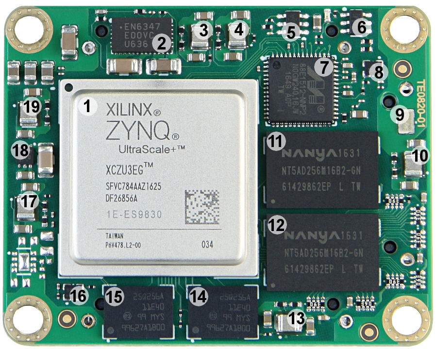
Figure 2: TE0820-02 main components.
- Xilinx Zynq UltraScale+ ZU3EG MPSoC, U1
- 4A PowerSoC DC-DC converter (PL_VCCINT, 0.85V), U5
- 3A high-efficiency step-down converter with integrated inductor (PS_AVCC, 0.9V), U9
- 3A high-efficiency step-down converter with integrated inductor (PS_AVTT, 1.8V), U13
3A load switch with configurable slew rate, fast transient isolation, hysteresis control (3.3V), Q1
- Ultra-low supply-current voltage monitor with optional watchdog, U19
- Marvell Alaska 88E1512 integrated 10/100/1000 Mbps energy efficient ethernet transceiver, U8
- Low-power programmable oscillator @ 12.000000 MHz, U11
- Miniature traceability S/N pad for low-cost, unique product identification
- 3A high-efficiency step-down converter with integrated inductor (DDR_2V5, 2.5V), U4
- 4 Gbit (256 x 16) DDR4 SDRAM, U3
- 4 Gbit (256 x 16) DDR4 SDRAM, U2
- 3A high-efficiency step-down converter with integrated inductor (DDR_1V2, 1.2V), U15
- 1.8V, 256 Mbit multiple I/O serial flash memory, U17
- 1.8V, 256 Mbit multiple I/O serial flash memory, U7
- Low-power programmable oscillator @ 33.333333 MHz, U32
- 3A high-efficiency step-down converter with integrated inductor (PS_VCCINT, 0.85V), U12
- 350 mA, ultra-low VIN, RF low-dropout linear regulator with bias pin (PS_PLL, 1.2V), U23
- 3A high-efficiency step-down converter with integrated inductor (1.8V), U20
- B2B connector Samtec Razor Beam™ LSHM-150, JM2
- DDR termination regulator with VTTREF buffered reference, U16
- Low-power programmable oscillator @ 52.000000 MHz, U14
- Highly integrated full featured hi-speed USB 2.0 ULPI transceiver, U18
- B2B connector Samtec Razor Beam™ LSHM-130, JM3
- I2C programmable, any frequency , any output quad clock generator, U10
- B2B connector Samtec Razor Beam™ LSHM-150, JM1
- Lattice Semiconductor MachXO2 System Controller CPLD, U21
- 4 GByte eMMC memory, U6
Initial Delivery State
| Storage Device Name | Content | Notes |
|---|---|---|
SPI Flash OTP Area | Empty, not programmed | Except serial number programmed by flash vendor. |
SPI Flash Quad Enable bit | Programmed | - |
SPI Flash main array | Not programmed | - |
eFUSE USER | Not programmed | - |
eFUSE Security | Not programmed | - |
| Si5338 OTP NVM | Not programmed | - |
| CPLD (LCMXO2-256HC) | SC0820-02 QSPI Firmware | See Boot Process section |
Table 1: Initial delivery state of programmable devices on the module.
Boot Process
Two different firmware versions are available, one with the QSPI boot option and other with the SD Card boot option.
| B2B JM1 MODE Pin | QSPI Firmware Version | SD Card Firmware Version |
|---|---|---|
| Low | JTAG | Boot from SD Card |
| High | Boot from Flash | JTAG |
Table 2: Boot mode pin description.
For more information refer to the TE0820 CPLD - BootMode section.
Signals, Interfaces and Pins
Board to Board (B2B) I/Os
Zynq MPSoC's I/O banks signals connected to the B2B connectors:
| Bank | Type | B2B Connector | I/O Signal Count | Voltage | Notes |
|---|---|---|---|---|---|
64 | HP | JM2 | 48 | User | Max voltage 1.8V. |
64 | HP | JM2 | 2 | User | Max voltage 1.8V. |
| 65 | HP | JM2 | 18 | User | Max voltage 1.8V. |
65 | HP | JM3 | 16 | User | Max voltage 1.8V. |
66 | HP | JM1 | 48 | User | Max voltage 1.8V. |
501 | MIO | JM1 | 6 | 1.8V | - |
505 | GTR | JM3 | 4 lanes | N/A | - |
505 | GTR CLK | JM3 | 1 differential input | N/A | - |
Table 3: General overview of board to board I/O signals.
For detailed information about the pin-out, please refer to the Pin-out table.
MGT Lanes
The Xilinx Zynq UltraScale+ device used on the TE0820 module has 4 GTR transceivers. All 4 are wired directly to B2B connector JM3. MGT (Multi Gigabit Transceiver) lane consists of one transmit and one receive (TX/RX) differential pairs, four signals total per one MGT lane. Following table lists lane number, FPGA bank number, transceiver type, signal schematic name, board-to-board pin connection and FPGA pins connection:
| Lane | Bank | Type | Signal Name | B2B Pin | FPGA Pin |
|---|---|---|---|---|---|
| 0 | 505 | GTR |
|
|
|
| 1 | 505 | GTR |
|
|
|
| 2 | 505 | GTR |
|
|
|
| 3 | 505 | GTR |
|
|
|
Table 4: MGT lanes.
There are 3 clock sources for the GTR transceivers. B505_CLK0 is connected directly to B2B connector JM3, so the clock can be provided by the carrier board. Clocks B505_CLK1 and B505_CLK3 are provided by the on-board clock generator (U10). As there are no capacitive coupling of the data and clock lines that are connected to the connectors, these may be required on the user’s PCB depending on the application.
| Clock signal | Bank | Source | FPGA Pin | Notes |
|---|---|---|---|---|
| B505_CLK0_P | 505 | B2B, JM3-31 | PS_MGTREFCLK0P_505, F23 | Supplied by the carrier board. |
| B505_CLK0_N | 505 | B2B, JM3-33 | PS_MGTREFCLK0N_505, F24 | Supplied by the carrier board. |
| B505_CLK1_P | 505 | U10, CLK2A | PS_MGTREFCLK1P_505, E21 | On-board Si5338A. |
| B505_CLK1_N | 505 | U10, CLK2B | PS_MGTREFCLK1N_505, E22 | On-board Si5338A. |
| B505_CLK2_P | 505 | N/A | PS_MGTREFCLK2P_505, C21 | Not connected. |
| B505_CLK2_N | 505 | N/A | PS_MGTREFCLK2N_505, C22 | Not connected. |
| B505_CLK3_P | 505 | U10, CLK1A | PS_MGTREFCLK3P_505, A21 | On-board Si5338A. |
| B505_CLK3_N | 505 | U10, CLK1B | PS_MGTREFCLK3N_505, A22 | On-board Si5338A. |
Table 5: MGT reference clock sources.
JTAG Interface
JTAG access to the Xilinx Zynq-7000 is provided through B2B connector JM2.
JTAG Signal | B2B Connector Pin |
|---|---|
| TMS | JM2-93 |
| TDI | JM2-95 |
| TDO | JM2-97 |
| TCK | JM2-99 |
Table 6: JTAG interface signals.
Pin 89 JTAGEN of B2B connector JM1 is used to control which device is accessible via JTAG. If set to low or grounded, JTAG interface will be routed to the Xilinx Zynq MPSoC. If pulled high, JTAG interface will be routed to the System Controller CPLD.
System Controller CPLD I/O Pins
Special purpose pins are connected to System Controller CPLD and have following default configuration:
| Pin Name | Mode | Function | Default Configuration |
|---|---|---|---|
| EN1 | Input | Power Enable | No hard wired function on PCB. When forced low, pulls up PGOOD, goes low without effect on power management. |
| PGOOD | Output | Power Good | Active high when all on-module power supplies are working properly. |
| NOSEQ | - | - | No function. |
| RESIN | Input | Reset | Active low reset, gated to POR_B. |
| JTAGEN | Input | JTAG Select | Low for normal operation, high for CPLD JTAG access. |
Table 7: System Controller CPLD special purpose pins.
See also TE0820 CPLD.
Default PS MIO Mapping
| PS MIO | Function | B2B Pin | Connected to | PS MIO | Function | B2B Pin | Connected to |
|---|---|---|---|---|---|---|---|
| 0 | SPI0 | - | U7-B2, CLK | 40..45 | - | - | Not connected |
| 1 | SPI0 | - | U7-D2, DO/IO1 | 46 | SD | JM1-17 | B2B, SD_DAT3 |
| 2 | SPI0 | - | U7-C4, WP/IO2 | 47 | SD | JM1-19 | B2B, SD_DAT2 |
| 3 | SPI0 | - | U7-D4, HOLD/IO3 | 48 | SD | JM1-21 | B2B, SD_DAT1 |
| 4 | SPI0 | - | U7-D3, DI/IO0 | 49 | SD | JM1-23 | B2B, SD_DAT0 |
| 5 | SPI0 | - | U7-C2, CS | 50 | SD | JM1-25 | B2B, SD_CMD |
| 6 | N/A | - | Not connected | 51 | SD | JM1-27 | B2B, SD_CLK |
| 7 | SPI1 | - | U17-C2, CS | 52 | USB_PHY | - | U18-31, OTG-DIR |
| 8 | SPI1 | - | U17-D3, DI/IO0 | 53 | USB_PHY | - | U18-31, OTG-DIR |
| 9 | SPI1 | - | U17-D2, DO/IO1 | 54 | USB_PHY | - | U18-5, OTG-DATA2 |
| 10 | SPI1 | - | U17-C4, WP/IO2 | 55 | USB_PHY | - | U18-2, OTG-NXT |
| 11 | SPI1 | - | U17-D4, HOLD/IO3 | 56 | USB_PHY | - | U18-3, OTG-DATA0 |
| 12 | SPI1 | - | U17-B2, CLK | 57 | USB_PHY | - | U18-4, OTG-DATA1 |
| 13..20 | eMMC | - | U6, MMC-D0..D7 | 58 | USB_PHY | - | U18-29, OTG-STP |
| 21 | eMMC | - | U6, MMC-CMD | 59 | USB_PHY | - | U18-6, OTG-DATA3 |
| 22 | eMMC | - | U6, MMC-CLKR | 60 | USB_PHY | - | U18-7, OTG-DATA4 |
| 23 | eMMC | - | U6, MMC-RST | 61 | USB_PHY | - | U18-9, OTG-DATA5 |
| 24 | ETH | - | U8, ETH-RST | 62 | USB_PHY | - | U18-10, OTG-DATA6 |
| 25 | USB_PHY | - | U18, OTG-RST | 63 | USB_PHY | - | U18-13, OTG-DATA7 |
| 26 | MIO | JM1-95 | B2B | 64 | ETH | - | U8-53, ETH-TXCK |
| 27 | MIO | JM1-93 | B2B | 65..66 | ETH | - | U8-50..51, ETH-TXD0..1 |
| 28 | MIO | JM1-99 | B2B | 67..68 | ETH | - | U8-54..55, ETH-TXD2..3 |
| 29 | MIO | JM1-99 | B2B | 69 | ETH | - | U8-56, ETH-TXCTL |
| 30 | MIO | JM1-92 | B2B | 70 | ETH | - | U8-46, ETH-RXCK |
| 31 | MIO | JM1-85 | B2B (UART RX) | 71..72 | ETH | - | U8-44..45, ETH-RXD0..1 |
| 32 | MIO | JM1-91 | B2B (UART TX) | 73..74 | ETH | - | U8-47..48, ETH-RXD2..3 |
| 33 | MIO | JM1-87 | B2B | 75 | ETH | - | U8-43, ETH-RXCTL |
| 38 | I2C | - | U10-12, SCL | 76 | ETH | - | U8-7, ETH-MDC |
| 39 | I2C | - | U10-19, SDA | 77 | ETH | - | U8-8, ETH-MDIO |
Table 8: TE0820-02 PS MIO mapping.
Gigabit Ethernet
On-board Gigabit Ethernet PHY is provided with Marvell Alaska 88E1512 chip. The Ethernet PHY RGMII interface is connected to the Zynq Ethernet0 PS GEM0. I/O voltage is fixed at 1.8V for HSTL signaling. SGMII (SFP copper or fiber) can be used directly with the Ethernet PHY, as the SGMII pins are available on the B2B connector JM3. The reference clock input of the PHY is supplied from an on-board 25MHz oscillator (U11), the 125MHz output clock is left unconnected.
Ethernet PHY connection
| PHY Pin | ZYNQ PS | ZYNQ PL | Notes |
|---|---|---|---|
| MDC/MDIO | MIO76, MIO77 | - | - |
| LED0 | - | K8 | Can be routed via PL to any free PL I/O pin in B2B connector. |
| LED1 | - | - | CPLD pin 17. |
| LED2 | - | - | Not connected. |
| CONFIG | - | - | Wired to the 1.8V. |
| RESETn | MIO24 | - | - |
| RGMII | MIO64..MIO75 | - | - |
| SGMII | - | - | Routed to the B2B connector JM3. |
Table 9: General overview of the Gigabit Ethernet PHY signals.
USB Interface
USB PHY is provided by Microchip USB3320. The ULPI interface is connected to the Zynq PS USB0. I/O voltage is fixed at 1.8V. Reference clock input for the USB PHY is supplied by the on-board 25.000000 MHz oscillator (U15).
USB PHY connection
| PHY Pin | ZYNQ Pin | B2B Name | Notes |
|---|---|---|---|
| ULPI | MIO52..63 | - | Zynq USB0 MIO pins are connected to the USB PHY. |
| REFCLK | - | - | 52.000000 MHz from on-board oscillator (U14). |
| REFSEL[0..2] | - | - | Reference clock frequency select, all set to GND selects 52.000000 MHz. |
| RESETB | MIO25 | - | Active low reset. |
| CLKOUT | MIO52 | - | Connected to 1.8V, selects reference clock operation mode. |
| DP, DM | - | OTG_D_P, OTG_D_N | USB data lines routed to B2B connector JM3 pins 47 and 49. |
| CPEN | - | VBUS_V_EN | External USB power switch active high enable signal, routed to JM3 pin 17. |
| VBUS | - | USB_VBUS | Connect to USB VBUS via a series of resistors, see reference schematics, routed to JM3 pin 55. |
| ID | - | OTG_ID | For an A-device connect to ground, for a B-device left floating. routed from JM3 pin 23. |
Table 10: General overview of the USB PHY signals.
I2C Interface
On-board I2C devices are connected to MIO38 (SCL) and MIO39 (SDA) which are configured as I2C1 by default. Addresses for on-board I2C slave devices are listed in the table below:
| I2C Device | I2C Address | Notes |
|---|---|---|
Si5338A PLL | 0x70 | - |
| EEPROM | 0x53 | - |
Table 11: Address table of the I2C bus slave devices.
On-board Peripherals
System Controller CPLD
The System Controller CPLD (U21) is provided by Lattice Semiconductor LCMXO2-256HC (MachXO2 product family). It is the central system management unit with module specific firmware installed to monitor and control various signals of the FPGA, on-board peripherals, I/O interfaces and module as a whole.
See also TE0820 System Controller CPLD page.
DDR4 Memory
By default TE0820-02 module has two 16-bit wide Nanya NT5AD256M16B2 DDR4 SDRAM chips arranged into 32-bit wide memory bus providing total of 1 GBytes of on-board RAM. Different memory sizes are available optionally.
Quad SPI Flash Memory
Two quad SPI compatible serial bus flash N25Q256A memory chips are provided for FPGA configuration file storage. After configuration completes the remaining free memory can be used for application data storage. All four SPI data lines are connected to the FPGA allowing x1, x2 or x4 data bus widths to be used. The maximum data transfer rate depends on the bus width and clock frequency.
Gigabit Ethernet PHY
On-board Gigabit Ethernet PHY (U8) is provided with Marvell Alaska 88E1512 IC (U8). The Ethernet PHY RGMII interface is connected to the ZynqMP Ethernet3 PS GEM3. I/O voltage is fixed at 1.8V for HSTL signaling. The reference clock input of the PHY is supplied from an on-board 25.000000 MHz oscillator (U21).
High-speed USB ULPI PHY
Hi-speed USB ULPI PHY (U32) is provided with USB3320 from Microchip. The ULPI interface is connected to the Zynq PS USB0 via MIO28..39, bank 501 (see also section). The I/O voltage is fixed at 1.8V and PHY reference clock input is supplied from the on-board 52.000000 MHz oscillator (U33).
MAC Address EEPROM
A Microchip 24AA025E48 serial EEPROM (U25) contains a globally unique 48-bit node address, which is compatible with EUI-48(TM) specification. The device is organized as two blocks of 128 x 8-bit memory. One of the blocks stores the 48-bit node address and is write protected, the other block is available for application use. It is accessible over I2C bus with slave device address 0x53.
Programmable Clock Generator
There is a Silicon Labs I2C programmable clock generator Si5338A (U10) chip on the module. It's output frequencies can be programmed using the I2C bus address 0x70 or 0x71. Default address is 0x70, IN4/I2C_LSB pin must be set to high for address 0x71.
A 25.000000 MHz oscillator is connected to the pin IN3 and is used to generate the output clocks. The oscillator has its output enable pin permanently connected to 1.8V power rail, thus making output frequency available as soon as 1.8V is present. Three of the Si5338 clock outputs are connected to the FPGA. One is connected to a logic bank and the other two are connected to the GTR banks. It is possible to use the clocks connected to the GTR bank in the user's logic design. This is achieved by instantiating a IBUFDSGTE buffer in the design.
Once running, the frequency and other parameters can be changed by programming the device using the I2C bus connected between the FPGA (master) and clock generator (slave). For this, proper I2C bus logic has to be implemented in FPGA.
| Signal | Frequency | Notes |
|---|---|---|
| IN1/IN2 | - | Not used (external clock signal supply). |
IN3 | 25.000000 MHz | Fixed input clock signal from reference clock generator SiT8008BI-73-18S-25.000000E (U11). |
| IN4 | - | LSB of the default I2C address, wired to ground mean address is 0x70. |
IN5 | - | Not connected. |
IN6 | - | Wired to ground. |
| CLK0 A/B | - | Bank 65 clock input, pins K9 and J9. |
CLK1 A/B | - | MGT reference clock 3 to FPGA Bank 505 MGT. |
CLK2 A/B | - | MGT reference clock 1 to FPGA Bank 505 MGT. |
| CLK3 A/B | - | Not connected. |
Table 12: General overview of the on-board quad clock generator I/O signals.
Oscillators
The module has following reference clock signals provided by on-board oscillators and external source from carrier board:
| Clock Source | Schematic Name | Frequency | Clock Destination |
|---|---|---|---|
| SiTime SiT8008BI oscillator, U21 | PS_CLK | 33.333333 MHz | Zynq MPSoC U1,pin R16 |
| SiTime SiT8008BI oscillator, U21 | - | 25.000000 MHz | Quad PLL clock generator U10, pin 3, and Ethernet PHY U8, pin 34 |
Table 13: Reference clock signals.
On-board LEDs
There is one on-board red LED D1 wired to the PS DONE signal.
Power and Power-on Sequence
Power Supply
Power supply with minimum current capability of 3A for system startup is recommended.
Power Consumption
| Power Input | Typical Current |
|---|---|
| VIN | TBD* |
| 3.3VIN | TBD* |
Table 14: Power consumption.
*TBD - To be determined.
Power Distribution Dependencies
Module has two power input rails which can be connected to the single power source.
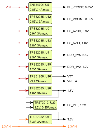
Figure 3: TE0820-02 power distribution diagram.
Power-On Sequence
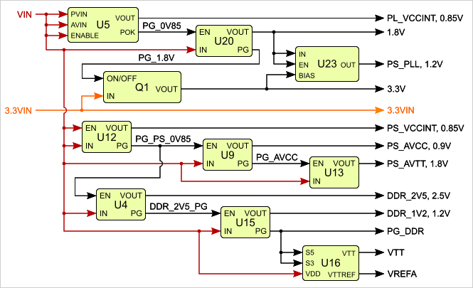
Figure 4: TE0820-02 power-on sequence diagram.
For highest efficiency of the on-board DC-DC regulators, it is recommended to use one 3.3V power source for both VIN and 3.3VIN power rails. Although VIN and 3.3VIN can be powered up in any order, it is recommended to power them up simultaneously.
It is important that all carrier board I/Os are 3-stated at power-on until System Controller CPLD sets PGOOD signal high (B2B connector JM1, pin 30), or 3.3V is present on B2B connector JM2 pins 10 and 12, indicating that all on-module voltages have become stable and module is properly powered up.
See Xilinx datasheet DS925 for additional information. User should also check related carrier board documentation when choosing carrier board design for TE0715 module.
Power Rails
| Power Rail Name on B2B Connector | JM1 Pins | JM2 Pins | Direction | Notes |
|---|---|---|---|---|
| VIN | 1, 3, 5 | 2, 4, 6, 8 | Input | Supply voltage from the carrier board. |
| 3.3V | - | 10, 12 | Output | Internal 3.3V voltage level. |
| 3.3VIN | 13, 15, 91 | - | Input | Supply voltage from the carrier board. |
| VCCO_64 | - | 7, 9 | Input | High performance I/O bank voltage. |
| VCCO_65 | - | 5 | Input | High performance I/O bank voltage. |
| VCCO_66 | 9, 11 | - | Input | High performance I/O bank voltage. |
Table 15: TE0820-02 power rails.
Bank Voltages
| Bank | Name on Schematic | Voltage | Range |
|---|---|---|---|
| 64 HP | VCCO_64 | User | HP: 1.0V to 1.8V |
| 65 HP | VCCO_65 | User | HP: 1.0V to 1.8V |
| 66 HP | VCCO_66 | User | HP: 1.0V to 1.8V |
| 500 PSMIO | VCCO_PSIO0_500 | 1.8V | - |
| 501 PSMIO | VCCO_PSIO1_501 | 3.3V | - |
| 502 PSMIO | VCCO_PSIO2_502 | 1.8V | - |
| 503 PSCONFIG | VCCO_PSIO3_503 | 1.8V | - |
| 504 PSDDR | VCCO_PSDDR_504 | 1.2V | - |
Table 16: TE0820-02 I/O bank voltages.
See Xilinx Zynq UltraScale+ datasheet DS925 for the voltage ranges allowed.
Board to Board Connectors
Unable to render {include} The included page could not be found.
Variants Currently In Production
Module Variant | MPSoC | RAM | SPI Flash | Temperature Range |
|---|---|---|---|---|
| TE0820-02-02CG-1E | XCZU2CG-1SFVC784E | 1 GByte DDR4 | 64 MByte | Extended |
| TE0820-02-03CG-1E | XCZU3CG-1SFVC784E | 1 GByte DDR4 | 64 MByte | Extended |
| TE0820-02-02EG-1E | XCZU2EG-1SFVC784E | 1 GByte DDR4 | 64 MByte | Extended |
| TE0820-02-03EG-1E | XCZU3EG-1SFVC784E | 1 GByte DDR4 | 64 MByte | Extended |
Table 17: TE0820-02 variants.
Technical Specifications
Absolute Maximum Ratings
Parameter | Min | Max | Units | Notes |
|---|---|---|---|---|
VIN supply voltage | -0.3 | 7.0 | V | See EN6347QI and TPS82085SIL datasheets. |
| 3.3VIN supply voltage | -0.1 | 3.75 | V | See LCMXO2-256HC and TPS27082L datasheet. |
| PS I/O supply voltage, VCCO_PSIO | -0.5 | 3.630 | V | Xilinx document DS925 |
| PS I/O input voltage | -0.5 | VCCO_PSIO + 0.55 | V | Xilinx document DS925 |
| HP I/O bank supply voltage, VCCO | -0.5 | 2.0 | V | Xilinx document DS925 |
| HP I/O bank input voltage | -0.55 | VCCO + 0.55 | V | Xilinx document DS925 |
Voltage on module JTAG pins | -0.4 | VCCO_0 + 0.55 | V | VCCO_0 is 1.8V or 3.3V nominal. Xilinx document DS925 |
Storage temperature | -40 | +85 | °C | See eMMC datasheet. |
Table 18: Module absolute maximum ratings.
Recommended Operating Conditions
| Parameter | Min | Max | Units | Notes |
|---|---|---|---|---|
| VIN supply voltage | 2.5 | 6.6 | V | See TPS82085S datasheet |
| 3.3VIN supply voltage | 2.375 | 3.6 | V | See LCMXO2-256HC datasheet |
| PS I/O supply voltage, VCCO_PSIO | 1.710 | 3.465 | V | Xilinx document DS925 |
| PS I/O input voltage | –0.20 | VCCO_PSIO + 0.20 | V | Xilinx document DS925 |
| HP I/O banks supply voltage, VCCO | 1.14 | 3.465 | V | Xilinx document DS925 |
| HP I/O banks input voltage | -0.20 | VCCO + 0.20 | V | Xilinx document DS925 |
| Voltage on module JTAG pins | 3.135 | 3.465 | V | For a module variant with 3.3V CONFIG bank option |
Table 19: Recommended operating conditions.
See Xilinx datasheet DS925 for more information about absolute maximum and recommended operating ratings for the Zynq UltraScale+ chips.
Operating Temperature Ranges
Extended grade: 0°C to +85°C.
Module operating temperature range depends also on customer design and cooling solution. Please contact us for options.
Physical Dimensions
Module size: 50 mm × 40 mm. Please download the assembly diagram for exact numbers.
Mating height with standard connectors: 8 mm
PCB thickness: 1.6 mm
Highest part on PCB: approximately 5 mm. Please download the step model for exact numbers.
All dimensions are shown in millimeters. Additional sketches, drawings and schematics can be found here.
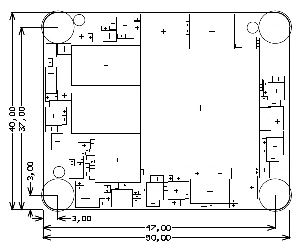
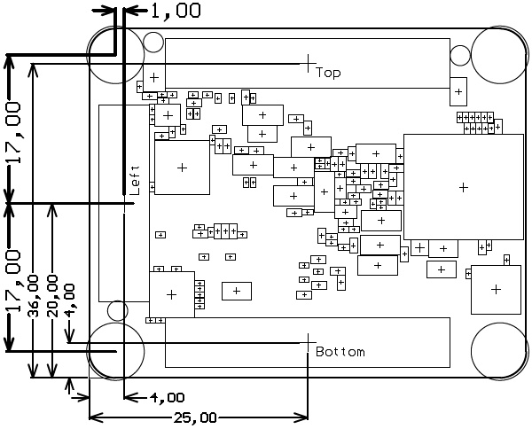
Figure 5: TE0820 module physical dimensions.
Revision History
Hardware Revision History
| Date | Revision | Notes | PCN Link | Documentation Link |
|---|---|---|---|---|
| 2017-08-17 | 02 | -- | TE0820-02 | |
| 2016-12-23 | 01 | Prototype only | TE0820-01 |
Table 20: Hardware revision history table.
Hardware revision number is written on the PCB board next to the module model number separated by the dash.
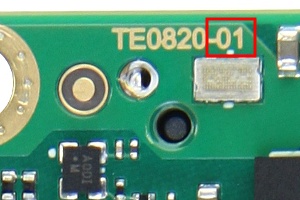
Figure 6: TE0820 module hardware revision.
Document Change History
Date | Revision | Contributors | Description |
|---|---|---|---|
| Jan Kumann | MGT lanes section added. | ||
2017-08-24 | v.36 | John Hartfiel | Correction in the "Key Features" section. |
| 2017-08-21 | v.34 | John Hartfiel | "Initial delivery state" section updated. |
| 2017-08-21 | v.33 | Jan Kumann |
|
2017-08-18 | v.7 | John Hartfiel |
|
2017-08-07 | v.5 | Jan Kumann | Initial version. |
Table 21: Document change history.
Disclaimer
Data Privacy
Please also note our data protection declaration at https://www.trenz-electronic.de/en/Data-protection-Privacy
Document Warranty
The material contained in this document is provided “as is” and is subject to being changed at any time without notice. Trenz Electronic does not warrant the accuracy and completeness of the materials in this document. Further, to the maximum extent permitted by applicable law, Trenz Electronic disclaims all warranties, either express or implied, with regard to this document and any information contained herein, including but not limited to the implied warranties of merchantability, fitness for a particular purpose or non infringement of intellectual property. Trenz Electronic shall not be liable for errors or for incidental or consequential damages in connection with the furnishing, use, or performance of this document or of any information contained herein.
Limitation of Liability
In no event will Trenz Electronic, its suppliers, or other third parties mentioned in this document be liable for any damages whatsoever (including, without limitation, those resulting from lost profits, lost data or business interruption) arising out of the use, inability to use, or the results of use of this document, any documents linked to this document, or the materials or information contained at any or all such documents. If your use of the materials or information from this document results in the need for servicing, repair or correction of equipment or data, you assume all costs thereof.
Copyright Notice
No part of this manual may be reproduced in any form or by any means (including electronic storage and retrieval or translation into a foreign language) without prior agreement and written consent from Trenz Electronic.
Technology Licenses
The hardware / firmware / software described in this document are furnished under a license and may be used /modified / copied only in accordance with the terms of such license.
Environmental Protection
To confront directly with the responsibility toward the environment, the global community and eventually also oneself. Such a resolution should be integral part not only of everybody's life. Also enterprises shall be conscious of their social responsibility and contribute to the preservation of our common living space. That is why Trenz Electronic invests in the protection of our Environment.
REACH, RoHS and WEEE
REACH
Trenz Electronic is a manufacturer and a distributor of electronic products. It is therefore a so called downstream user in the sense of REACH. The products we supply to you are solely non-chemical products (goods). Moreover and under normal and reasonably foreseeable circumstances of application, the goods supplied to you shall not release any substance. For that, Trenz Electronic is obliged to neither register nor to provide safety data sheet. According to present knowledge and to best of our knowledge, no SVHC (Substances of Very High Concern) on the Candidate List are contained in our products. Furthermore, we will immediately and unsolicited inform our customers in compliance with REACH - Article 33 if any substance present in our goods (above a concentration of 0,1 % weight by weight) will be classified as SVHC by the European Chemicals Agency (ECHA).
RoHS
Trenz Electronic GmbH herewith declares that all its products are developed, manufactured and distributed RoHS compliant.
WEEE
Information for users within the European Union in accordance with Directive 2002/96/EC of the European Parliament and of the Council of 27 January 2003 on waste electrical and electronic equipment (WEEE).
Users of electrical and electronic equipment in private households are required not to dispose of waste electrical and electronic equipment as unsorted municipal waste and to collect such waste electrical and electronic equipment separately. By the 13 August 2005, Member States shall have ensured that systems are set up allowing final holders and distributors to return waste electrical and electronic equipment at least free of charge. Member States shall ensure the availability and accessibility of the necessary collection facilities. Separate collection is the precondition to ensure specific treatment and recycling of waste electrical and electronic equipment and is necessary to achieve the chosen level of protection of human health and the environment in the European Union. Consumers have to actively contribute to the success of such collection and the return of waste electrical and electronic equipment. Presence of hazardous substances in electrical and electronic equipment results in potential effects on the environment and human health. The symbol consisting of the crossed-out wheeled bin indicates separate collection for waste electrical and electronic equipment.
Trenz Electronic is registered under WEEE-Reg.-Nr. DE97922676.
Overview
Content Tools