Table of Contents
Overview
The Trenz Electronic TEC0330 FPGA board is a PCI Express form factor card (PCIe 2.0 or higher) integrating the Xilinx Virtex-7 XC7VX330T FPGA chip. This high-end FPGA card is designed for maximum system performance and intended for use in applications with high demands on system throughput. There is a SO-DIMM socket on the board for standard DDR3 SDRAM extension memory module.
The TEC0330 features HPC (High Pin Count) ANSI/VITA 57.1 compatible FMC interface connector for standard I/O Mezzanine modules. Other interface connectors found on-board include JTAG for accessing FPGA and on-board System Controller CPLD, and also connector with 5 high-speed I/O differential signaling pairs.
The TEC0330 FPGA board is intended to be used as add-on card in a PCIe 2.0 or higher capable host systems, it can not be used as a stand-alone device.
Key Features
- Xilinx Virtex-7 FPGA module XC7VX330T-2FFG1157C (commercial temperature range)
- PCI Express 2.0 x8 card with maximum throughput of 4 GB/s
- FMC High Pin Count (HPC) connector
- 8 FPGA MGT lanes available on PCIe interface
- DDR3 SO-DIMM SDRAM socket
- 256-Mbit (32-MByte) Quad SPI Flash memory (for configuration and operation) accessible through:
- FPGA
- JTAG port (SPI indirect, bus width x4)
- External clock input via SMA coaxial connector
- 28 GTH transceivers, each with up to 13.1 Gbit/s data transmission rate
- FPGA configuration through:
- JTAG connector
- SPI Flash memory
- Programmable quad clock generator
- TI LMK04828B ultra low-noise JESD204B compliant clock jitter cleaner
- On-board high-efficiency DC-DC converters
- Up to 202 FPGA I/O pins available on FMC connector (up to 101 LVDS pairs possible)
- System management and power sequencing
- AES bit-stream encryption
- eFUSE bit-stream encryption
Additional assembly options are available for cost or performance optimization upon request.
Block Diagram
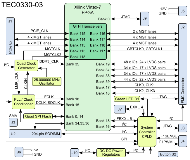
Figure 1: TEC0330-03 Block Diagram.
Main Components
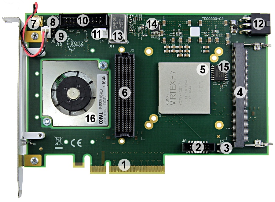
Figure 2: FPGA board TEC0330-03.
- PCI Express 2.0 x8 connector, J1
- FPGA JTAG connector, J9
- User button, S2
- SO-DIMM socket, U2
- Xilinx Virtex-7 XC7VX330T-2FFG1157C FPGA, U1
- ANSI/VITA 57.1 compliant FMC HPC connector, J2
- SMA coaxial connector for external clock input, J3
- System Controller CPLD JTAG connector, J8
- I2C connector for LT LTM4676 step-down DC-DC regulator, J10
- IDC header for access to 5 x high-speed data lanes (LVDS pairs), J7
- 4-wire PWM fan connector, J4
- 6-pin 12V power connector, J5
- Reference clock generator @10.0 MHz (P5146) , U11
- LDO DC-DC regulator @3.3V (LMK_3V3) (TI TPS74901RGWR), U21
- 256 Mbit Quad SPI Flash Memory (Micron N25Q256A), U12
- Cooling fan 5VDC M1 (45X5MM, 0.7W, 1.06CFM)
- System Controller CPLD (Lattice Semiconductor LCMXO2-1200HC), U5
- Ultra low jitter clock synthesizer (TI LMK04828B), U9
- Step-down DC-DC regulator @1.0V (LT LTM4676), U4
- Step-down DC-DC regulator @1.5V (VCC1V5) (LT LTM4676, U3
- I2C Programmable quad clock generator (Silicon Labs Si5338A), U13
- 4A PowerSoC DC-DC converter @1.8V (Altera EN6347QI, U20
- LDO DC-DC regulator @1.0V (MGTAVCC_FPGA) (TI TPS74401RGW), U18
- LDO DC-DC regulator @1.2V (MGTAVTT_FPGA) (TI TPS74401RGW), U17
- 4A PowerSoC DC-DC converter @3.3V (3V3FMC) (Altera EN6347QI), U15
- 4A PowerSoC DC-DC converter @1.8V (FMC_VADJ) (Altera EN6347QI), U7
Initial Delivery State
| Storage device name | Content | Notes |
|---|---|---|
SPI Flash OTP Area | Empty, not programmed | Except serial number programmed by flash vendor. |
SPI Flash Quad Enable bit | Programmed | - |
SPI Flash main array | Demo design | - |
eFUSE USER | Not programmed | - |
eFUSE Security | Not programmed | - |
Table 1: Initial delivery state.
Signals, Interfaces and Pins
FMC Connector
The high-pin count (HPC) FMC (FPGA Mezzanine Card) connector (J2) is a standard ANSI/VITA 57.1 modular interface to the FPGA and provides access to numerous FPGA I/O pins for use by other mezzanine modules and expansion cards. The FMC connector supports single ended I/O (with several VCCIO voltages available) and LVDS I/O signaling.
The I/O signals are routed from the FPGA I/O banks to the FMC connector as LVDS pairs:
| Bank | I/O Signals | LVDS pairs | VCCO Bank Voltage | Notes |
|---|---|---|---|---|
| Bank 19 | 92 | 46 | 1.8V | - |
| Bank 39 | 42 | 21 | VIO_B_FMC | Bank voltage VIO_B_FMC must be supplied by FMC connector pins J2-J39, J2-K40 Bank's VREF_B_M2C signal is routed to the FMC connector pin J2-K1 (external reference voltage) |
| Bank 37 | 34 | 17 | 1.8V | Bank's VREF_A_M2C signal is routed to the FMC connector pin J2-H1 (external reference voltage) |
| Bank 38 | 34 | 17 | 1.8V | Bank's VREF_A_M2C signal is routed to the FMC connector pin J2-H1 (external reference voltage) |
Table 2: Overview of the FPGA I/O bank signals routed to the FMC.
There are also 10 high-speed MGT lanes (Xilinx GTH transceivers) from different FPGA MGT banks routed to the FMC connector.
The MGT banks have also clock input pins which are exposed to the FMC connector. Following MGT lanes are available on the FMC connector:
| FPGA Bank | I/O signals | LVDS pairs | MGT lanes | Bank's reference clock (LVDS pair) |
|---|---|---|---|---|
| 116 | 10 | 5 | 2 | 1 clock-signal from clock synthesizer U9 to bank's pins T6/T5 |
| 117 | 20 | 10 | 4 | 2 clock-signals from clock FMC connector GBTCLK0_M2C and GBTCLK1_M2C (pins J2-D4/J2-D5 and J2-B20/J2-B21) to bank's pins M6/M5 and P6/P5 |
| 118 | 20 | 10 | 4 | 1 reference clock from clock synthesizer U9 to bank's pins F6/F5 1 reference clock from programmable quad clock generator U13 to bank's pins H6/H5 |
Table 3: Overview of MGT banks lanes routed to the FMC connector.
The FMC connector provides JTAG and I2C interfaces to the System Controller CPLD:
| Interface | I/O signals | Schematic name / FMC pin | Connected to | Notes |
|---|---|---|---|---|
| JTAG | 5 | FMC_TRST, pin D34 FMC_TCK, pin D29 FMC_TMS, pin D33 FMC_TDI, pin D30 FMC_TDO, pin D31 | SC CPLD, bank 2 | VCCIO: 3V3PCI |
| I2C | 2 | FMC_SCL, pin C30 FMC_SDA, pin C31 | SC CPLD, bank 2 | VCCIO: 3V3PCI I2C-lines 3V3PCI pulled-up |
| Control lines | 3 | FMC_PRSNT_M2C_L, pin H2 FMC_PG_C2M, pin D1 (3V3FMC pull-up) FMC_PG_M2C, pin F1 (3V3FMC pull-up) | SC CPLD, bank 1 | PG - Power Good signal C2M - carrier to mezzanine module M2C - mezzanine module to carrier Internal System Controller CPLD signal assignment: FEX_0_N <= FMC_PG_M2C FMC_PG_C2M <= FMC_PRSNT_M2C_L |
Table 4: FMC connector pin-outs of available interfaces to the System Controller CPLD.
FPGA bank 17 and 18 clock inputs from FMC connector:
| Schematic name | FMC connector pins | FPGA bank | FPGA pins |
|---|---|---|---|
| CLK0_P, CLK0_N | H4, H5 | 17 | R28, R29 |
| CLK1_P, CLK1_N | G2, G3 | 17 | P29, P30 |
| CLK2_P, CLK2_N | K4, K5 | 18 | G31, G31 |
| CLK3_P, CLK3_N | J2, J3 | 18 | H29, H30 |
Table 5: FMC connector pin-outs for reference clock input.
Several VCCIO voltages are available on the FMC connector for FPGA I/O banks:
| Schematic name | Max current | FMC connector pins | Notes |
|---|---|---|---|
| 12V | 1A | C35/C37 | Externally supplied 12V |
| 3V3PCI | 20mA | D32 | Supplied by the PCIe interface |
| 3V3FMC | 3A | D36/D38/D40/C39 | Supplied by DC-DC converter U15 |
| VIO_B_FMC | External supply | J39/K40 | Externally supplied VCCO to HB FPGA bank 39 |
| FMC_VADJ | 4A | H40/G39/F40/E39 | Fixed to 1.8V, supplied by DC-DC converter U7 |
Table 6: Available VCCIO voltages on FMC connector.
PCI Express Interface
The TEC0330 FPGA board is also a PCI Express card designed to fit in computing systems with PCI Express x8 slots (PCIe 2.0 or higher) and is PCIe Gen. 2 capable.
8 MGT lanes are routed to the PCIe interface composed of RX/TX LVDS pairs for each lane:
| FPGA bank | I/O signal count | LVDS pairs | MGT lanes | Bank's reference clock (LVDS pair) |
|---|---|---|---|---|
| 114 | 16 | 8 | 4 | - |
| 115 | 18 | 9 | 4 | 1 reference clock from programmable quad clock generator 1 reference clock from PCIe interface J1 to bank's pins AD6/AD5 |
Table 7: MGT lanes available on PCIe interface.
MGT Lanes
MGT (Multi Gigabit Transceiver) lane consists of one receive and one transmit (RX/TX) differential pairs, four signals total per one MGT lane. Following table lists lane number, MGT bank number, transceiver type, signal schematic name, FMC connector pin connection and FPGA pin connection information:
FPGA to FMC MGT lanes
| Lane | Bank | Type | Signal Name | FMC Pin | FPGA Pin |
|---|---|---|---|---|---|
| 0 | 117 | GTH |
|
|
|
| 1 | 117 | GTH |
|
|
|
| 2 | 117 | GTH |
|
|
|
| 3 | 117 | GTH |
|
|
|
| 4 | 118 | GTH |
|
|
|
| 5 | 118 | GTH |
|
|
|
| 6 | 118 | GTH |
|
|
|
| 7 | 118 | GTH |
|
|
|
| 8 | 116 | GTH |
|
|
|
| 9 | 116 | GTH |
|
|
|
Table 8: FPGA to FMC connector MGT lanes overview (continue on next page).
FPGA to FMC MGT lanes (continued)
| Lane | Bank | Type | Signal Name | FMC Pin | FPGA Pin |
|---|---|---|---|---|---|
| 5 | 118 | GTH |
|
|
|
| 6 | 118 | GTH |
|
|
|
| 7 | 118 | GTH |
|
|
|
| 8 | 116 | GTH |
|
|
|
| 9 | 116 | GTH |
|
|
|
Table 8: FPGA to FMC connector MGT lanes overview.
JTAG Interfaces
TEC0330 board JTAG interfaces accessing the FPGA or the System Controller CPLD:
| JTAG interface | JTAG signals schematic name | JTAG connector pins | Connected to |
|---|---|---|---|
CPLD JTAG VCCIO: 3V3PCI Connector: J8 | CPLD_JTAG_TMS | J8-1 | SC CPLD, bank 0, pin 90 |
| CPLD_JTAG_TDI | J8-2 | SC CPLD, bank 0, pin 94 | |
| CPLD_JTAG_TDO | J8-3 | SC CPLD, bank 0, pin 95 | |
| CPLD_JTAG_TCK | J8-4 | SC CPLD, bank 0, pin 91 | |
FPGA JTAG VCCIO: 1V8 Connector: J9 | FPGA_JTAG_TMS | J9-4 | FPGA, bank 0, pin N9 |
| FPGA_JTAG_TCK | J9-6 | FPGA, bank 0, pin M8 | |
| FPGA_JTAG_TDO | J9-8 | FPGA, bank 0, pin N8 | |
| FPGA_JTAG_TDI | J9-10 | FPGA, bank 0, pin L8 | |
FMC JTAG VCCIO: 3.3VPCI Connector: J2 | FMC_TRST | J2-D34 | SC CPLD, bank 2, pin 36 |
| FMC_TCK | J2-D29 | SC CPLD, bank 2, pin 27 | |
| FMC_TMS | J2-D33 | SC CPLD, bank 2, pin 28 | |
| FMC_TDI | J2-D30 | SC CPLD, bank 2, pin 31 | |
| FMC_TDO | J2-D31 | SC CPLD, bank 2, pin 32 |
Table 9: JTAG Interface on TEC0330 board.
SO-DIMM Socket for DDR3 SDRAM
The TEC0330 board supports additional DDR3 SO-DIMM (204-pin) via 204-pin SO-DIMM socked U2. The DDR3 memory interface is routed to the FPGA banks 34, 35 and 36.
The reference clock signal for the DDR3 interface is generated by the quad programmable reference clock U13 and is applied to bank 35.
There is also a I2C interface between the System Controller CPLD and the DDR3 SDRAM memory:
| Interface signals schematic name | System Controller CPLD pin | DDR3 memory interface pin |
|---|---|---|
| DDR3_SDA | Bank 2, pin 48 | Pin 200 (3V3PCI pull-up) |
| DDR3_SCL | Bank 2, pin 49 | Pin 202 (3V3PCI pull-up) |
Table 10: I2C-interface between SC CPLD and DDR3 SDRAM memory.
System Controller CPLD
The System Controller CPLD is the central system management unit that provides numerous interfaces between the on-board peripherals and to the FPGA module. The signals routed to the CPLD will be linked by the logic implemented in the CPLD firmware, which generates output signals to control the system, the on-board peripherals and the interfaces. So some interfaces between the on-board peripherals and to the FPGA module are by-passed, forwarded and controlled by the System Controller CPLD.
Other tasks of the System Controller CPLD are the monitoring of the power-on sequence, the proper programing of the FPGA module and to display its programming state.
| CPLD bank | CPLD bank's VCCIO |
|---|---|
| 0 | 3V3PCI |
| 1 | 3V3PCI |
| 2 | 3V3PCI |
| 3 | 1V8 |
Table 11: VCCIO voltages of CPLD banks.
Following table describes the interfaces and functionalities of the System Controller CPLD, which are not described elsewhere in this TRM:
| CPLD functionality | Interface | Designated CPLD pins | Connected to | Notes |
|---|---|---|---|---|
| I2C interface between on-board peripherals and FPGA | I2C | FPGA_IIC_SDA, pin 24 FPGA_IIC_SCL, pin 25 FPGA_IIC_OE, pin 19 | FPGA bank 16, pin V29 FPGA bank 16, pin W29 FPGA bank 16, pin W26 | VCCIO: 1V8, all with pull-up to 1V8. Following devices and connectors are linked to the FPGA_IIC I2C interface:
Note: FPGA_IIC_OE must kept high for I2C operation. For I2C slave device addresses refer to the component datasheets. |
User I/Os External LVDS pairs | 10 I/Os 5 x differential signaling pairs | EX0_P ... EX4_P EX0_N ... EX4_N | IDC header J7 | Can also be used for single-ended signaling. |
User I/Os Internal LVDS pairs | 13 I/Os 6 x differential signaling pairs | FEX0_P ... FEX5_P FEX0_N ... FEX5_N FEX_DIR (single-ended I/O) | FPGA bank 18 | VCCIO: 1V8 Can also be used for single-ended signaling. FPGA bank 18 has also reference clock input from FMC connector (CLK2, CLK3) and clock synthesizer U9 (FCLK). Internal signal assignment: FEX_DIR <= FMC_PRSNT_M2C_L |
| FPGA programming control and state | 2 I/Os | DONE, pin 7 PROGRAM_B, pin 8 | FPGA bank 0, pin V8 FPGA bank 0, pin U8 | VCCIO: 1V8 |
| I2C interface to programmable quad clock generator | I²C | PLL_SCL, pin 14 PLL_SDA, pin 15 | U13, pin 12 U13, pin 19 | VCCIO: 1V8 Only PLL_SDA has 1V8 pull-up. |
| Fan PWM control J4 | 2 I/Os | F1SENSE, pin 99 F1PWM, pin 98 | J4-3 (active low) J4-4 | Internal signal assignment: FEX_5_P <= F1SENSE FEX_5_N => F1PWM |
| Button S2 | 1 I/O | BUTTON, pin 77 | Switch S2 | Functionality depends on CPLD firmware, activating pin PROGRAM_B (active low) and LED1 in standard configuration. |
| LED1 | 1 I/O | LED1, pin 76 | LED D1 (green) | Fast blinking, when FPGA is not programmed. Internal signal assignment: LED1 <= Button S2 or FEX0_P |
PCIe control line RESET_B | 1 I/O | PCIE_RSTB, pin 37 | PCIe connector J1-A11 (33R serial resistor) | Internal signal assignment: FEX_4_N <= PCIE_RSTB |
Control Interface to clock synthesizer U9 (TI LMK04828B) | SPI (3 I/Os), 4 I/Os | CLK_SYNTH_SDIO, pin 75 CLK_SYNTH_SCK, pin 74 CLK_SYNTH_RESET, pin 54 CLK_SYNTH_CS, pin 53 CLK_SYNTH_SYNC, pin 52 LMK_STAT0, pin 62 LMK_STAT1, pin 63 | U9, pin 20 U9, pin 19 U9, pin 5 U9, pin 18 U9, pin 6 U9, pin 31 U9, pin 48 | Pull up to 3V3PCI. Internal signal assignment: LMK_SCK <= FEX_1_P LMK_SDIO <= FEX_1_N LMK_CS <= FEX_3_P LMK_SYNC <= EX_3_N LMK_RESET <= FEX_4_P FEX_2_P => LMK_SDIO (FEX_2_N must be 0) LMK_STAT0 and LMK_STAT1 signals are not used. |
| Control Interface to DC-DC converters U3 and U4 (both LT LTM4676) | I2C (2 I/Os), 2 I/Os | LTM_SCL, pin 67 LTM_SDA, pin 66 LTM1_ALERT, pin 65 LTM2_ALERT, pin 64 | U4, pin E6 and U3, pin E6 U4, pin D6 and U3, pin D6 U4, pin E5 U3, pin E5 | 3V3 pull-ups. LTM I2C interface is also accessible trough header J10. LTM1_Alert and LTM2_ALERT signals are not used. |
| Power-on sequence and monitoring | 6 I/Os | EN_1V8, pin 58 PG_1V8, pin 59 EN_FMC_VADJ, pin 60 PG_FMC_VADJ, pin 61 EN_3V3, pin 51 PG_3V3, pin 57 | U20, pin 27 U20, pin 28 U7, pin 27 U7, pin 28 U15, pin 27 U15, pin 28 | Sequence of the supply voltages depend on the System Controller CPLD firmware. EN_1V8, EN_3V3 and EN_FMC_VADJ will be set simultaneously at start-up. PG signals will not be evaluated. |
Table 12: Overview of the System Controller CPLD functions.
Clocking
The TEC0330 FPGA board has a sophisticated clock generation and conditioning system to meet the requirements of the Xilinx Virtex-7 GTH units with data transmission rates up to 13.1 Gb/s.
Clock sources
List of on-board and external reference clock signals of the TE0330 board:
| Clock Source | Schematic Name | Frequency | Clock destination |
|---|---|---|---|
| SMA coaxial connector, J3 | CLK_SYNTH_CLKIN0_P, CLK_SYNTH_CLKIN0_N (GND) | User | Clock synthesizer U9, pins 37/38 |
| RAKON P5146LF oscillator, U11 | - | 10.0 MHz | Clock synthesizer U9, pins 43/44 |
| SiTime SiT8208 oscillator, U14 | CLK_25MHz | 25.0 MHz | Programmable quad clock generator U13, pin 3 |
| FMC connector J2, pins H4/H5 | CLK0_P, CLK0_N | User | FPGA bank 17, pins R28/R29 |
| FMC connector J2, pins G2/G3 | CLK1_P, CLK1_N | User | FPGA bank 17, pins P29/P30 |
| FMC connector J2, pins K4/K5 | CLK2_P, CLK2_N | User | FPGA bank 18, pins G30/G31 |
| FMC connector J2, pins J2/J3 | CLK3_P, CLK3_N | User | FPGA bank 18, pins H29/H30 |
| FMC connector J2, pins D4/D5 | GBTCLK0_M2C_P, GBTCLK0_M2C_N | User | FPGA bank 117, pins M6/M5 |
| FMC connector J2, pins B20/B21 | GBTCLK1_M2C_P, GBTCLK1_M2C_N | User | FPGA bank 117, pins P6/P5 |
| PCIe interface J1, pins A13/A14 | PCIE_CLK_P, PCIE_CLK_N | 100 MHz (PCIe spec.) | FPGA bank 115, pins AD6/AD5 |
Table 13: Clock generator sources overview.
Programmable Clock Generator
There is a Silicon Labs I2C programmable quad clock generator Si5338A (U13) on-board. It's output frequencies can be programmed by using the I2C-bus with address 0x70.
A 25 MHz (U14) oscillator is connected to pin 3 (IN3) and is used to generate the output clocks.
Once running, the frequency and other parameters can be changed by programming the device using the I2C bus connected between the FPGA (master) and clock generator (slave). Logic needs to be generated inside the FPGA module to utilize I²C-bus correctly.
| Si5338A (U13) input | Signal schematic name | Notes |
|---|---|---|
IN1/IN2 | CLKIN_5338_C_P, CLKIN_5338_C_N | Reference clock signal from clock synthesizer U9 (100 nF decoupling capacitors and 100Ω termination resistor) |
IN3 | Reference clock oscillator input, SiTime SiT8208AI (U14). | 25.0 MHz fixed frequency |
IN4/IN6 | Connected to the GND. | LSB (pin 'IN4') of the default I²C-adress 0x70 is zero |
IN5 | Not connected | - |
| Si5338A (U13) output | Signal schematic name | Notes |
CLK0 A/B | DDR3_CLK_P, DDR3_CLK_N | DDR3-RAM reference clock signal to FPGA bank 35 |
CLK1 A/B | MGTCLK_5338_C_P, MGTCLK_5338_C_N | Reference clock signal to FPGA bank 115 MGT (100 nF decoupling capacitors and 100Ω termination resistor) |
CLK2 A/B | LMK_CLK_P, LMK_CLK_N | Input clock signal to clock synthesizer U9 (100 nF decoupling capacitors) |
| CLK3 A/B | MGTCLK2_5338_C_P, MGTCLK2_5338_C_N | Reference clock signal to FPGA bank 118 MGT (100 nF decoupling capacitors and 100Ω termination resistor) |
Table 14: I/O pin description of programmable clock generator Si5338A.
Ultra low-noise high-performance clock synthesizer
The TEC0330 board utilizes an ultra low jitter clock synthesizer TI LMK04828B (U9) for conditioning and generating clean clock signals which are necessary for the GTH units of the Xilinx Virtex-7 FPGA module.
The clock synthesizer can be controlled and programmed by its SPI interface (SPI slave) and other control lines, which are routed to the FPGA module (SPI master) and by-passed trough the System Controller CPLD. See section 'System Controller CPLD' for more detailed information.
Logic needs to be generated inside the FPGA module to utilize SPI bus correctly.
| LMK04828B (U9) input | signal schematic name | Note |
|---|---|---|
| Status_LD1, Status_LD2 | LMK_STAT0, LMK_STAT1 | Connected to System Controller CPLD, not implemented in current CPLD firmware |
SPI interface and control lines | see section 'System controller CPLD' | The clock synthesizer can be controlled and programmed by the FPGA module via the SPI interface and control lines, which are by-passed through the System Controller CPLD |
| CLKin0, CLKin0* | CLK_SYNTH_CLKIN0_P, CLK_SYNTH_CLKIN0_N | Input reference clock signal via SMA coaxial connector J3, connected to CLKin0* via serial decoupling capacitor 100nF. CLKin0 to connected to GND via serial decoupling capacitor 100nF. |
| CLKin1, CLKin1* | CLK_SYNTH_CLKIN1_P, CLK_SYNTH_CLKIN1_N | Input reference clock signal from programmable quad clock generator Si5338A (U13) via serial decoupling capacitor 100nF. |
| OSCin, OSCin* | - | Signal from reference clock oscillator RAKON P51446LF, fixed to 10.0 MHz |
| LMK04828B (U9) output | signal schematic name | Note |
| DCLKout0, DCLKout0* | CLK_SYNTH_DCLKOUT0_P, CLK_SYNTH_DCLKOUT0_N | Reference clock signal to FPGA bank 15 pins AD29/AE29 |
| SDCLKout1, SDCLKout1* | CLK_SYNTH_SDCLKOUT1_P, CLK_SYNTH_SDCLKOUT1_N | Reference clock signal to FPGA bank 15 pins AE31/AF31 |
| DCLKout2, DCLKout2* | CLKIN_5338_P, CLKIN_5338_N | Reference clock signal to programmable quad clock generator Si5338A (U13) (100 nF decoupling capacitors and 100Ω termination resistor) |
| DCLKout4, DCLKout4* | CLK_SYNTH_DCLKOUT4_P, CLK_SYNTH_DCLKOUT4_N | Reference clock signal to FPGA bank 115 MGT, pins T6/T5 |
| SDCLKout7, SDCLKout7* | CLK_SYNTH_SDCLKOUT7_P, CLK_SYNTH_SDCLKOUT7_N | Reference clock signal to FPGA bank 118 MGT, pins F6/F5 |
| OSCout0, OSCout0* | CLK_SYNTH_CLKIN2_P, CLK_SYNTH_CLKIN2_N | Reference clock signal to FPGA bank 18, pins J30/J31 (100 nF decoupling capacitors) |
Table 15: Pin description of clock synthesizer TI LMK04828B.
32 MByte Quad SPI Flash Memory
An 256 Mbit (32 MByte) Quad SPI Flash Memory (Micron N25Q256A, U12) is provided for FPGA configuration file storage. After configuration process completes the remaining free memory can be used for application data storage. All four SPI data lines are connected to the FPGA allowing x1, x2 or x4 data bus widths to be used. The maximum data transfer rate depends on the bus width and clock frequency. The memory can be accessed indirectly by the FPGA JTAG port (J9) by implementing the functional logic for this purpose inside the FPGA.
Power and Power-On Sequence
Power Supply
6-pin 12V power connector J5 is the main power supply of the TEC0330 FPGA board, minimum current capability of 3A for system startup is recommended.
Power Consumption
| Power Input | Typical Current |
|---|---|
| 12V (J5) | TBD |
| 3V3PCI (J1) | TBD |
Table 16: Maximum current of power supplies. TBD - To Be Determined.
Power-On Sequence
The on-board voltages of the TEC0330 FPGA board will be powered up in order of a determined sequence after the external voltages 12V on connector J5 and 3V3PCI on connector J1 are available.
Core voltages and main supply voltages have to reach stable state and their "Power Good"-signals have to be asserted before other voltages like PL bank's I/O voltages can be powered up.
Following diagram describes the sequence of enabling the on-board voltages:
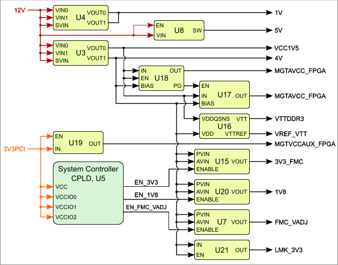
Figure 3: FPGA board TEC0330-03 power-on sequence diagram.
Bank Voltages
| Bank | Schematic Name | Voltage | Range | Note |
|---|---|---|---|---|
| 0 | 1V8 | 1.8V | HP: 1.2V to 1.8V | Config bank (fixed to 1.8V) / JTAG interface |
| 14 | 1V8 | 1.8V | HP: 1.2V to 1.8V | QSPI flash memory interface |
| 15 | 1V8 | 1.8V | HP: 1.2V to 1.8V | Reference clock input |
| 16 | 1V8 | 1.8V | HP: 1.2V to 1.8V | I2C interface of FPGA |
| 17 | 1V8 | 1.8V | HP: 1.2V to 1.8V | Reference clock input |
| 18 | 1V8 | 1.8V | HP: 1.2V to 1.8V | Reference clock input / I/O's to CPLD |
| 34 | VCC1V5 | 1.5V | HP: 1.2V to 1.8V | DDR3 memory interface |
| 35 | VCC1V5 | 1.5V | HP: 1.2V to 1.8V | DDR3 memory interface |
| 36 | VCC1V5 | 1.5V | HP: 1.2V to 1.8V | DDR3 memory interface |
114 115 116 117 118 | MGTAVCC_FPGA MGTVCCAUX_FPGA MGTAVTT_FPGA | 1.0V 1.8V 1.2V | MGT bank supply voltage MGT bank auxiliary supply voltage MGT bank termination circuits voltage | MGT banks with Xilinx GTH transceiver units |
| 19 | 1V8 | 1.8V | HP: 1.2V to 1.8V | I/Os routed to FMC, usable as LVDS pairs |
| 37 | 1V8 | 1.8V | HP: 1.2V to 1.8V | I/Os routed to FMC, usable as LVDS pairs |
| 38 | 1V8 | 1.8V | HP: 1.2V to 1.8V | I/Os routed to FMC, usable as LVDS pairs |
| 39 | VIO_B_FMC | user | HP: 1.2V to 1.8V | I/Os routed to FMC, usable as LVDS pairs |
Table 17: Range of FPGAs bank voltages.
See Xilinx Virtex-7 datasheet (DS183) for the voltage ranges allowed.
Power Rails
| Connector / Pin | Voltage | Direction | Notes |
|---|---|---|---|
| J4, pin 2 | 12V (filtered) | Output | 4-wire PWM fan connector supply voltage |
| J6, pin 2 | 5V (filtered) | Output | Cooling fan M1 supply voltage |
| J8, pin 6 | 3V3PCI | Output | VCCIO CPLD JTAG |
| J9, pin 2 | 1V8 | Output | VCCIO FPGA JTAG |
| J2, pin C35 / C37 | 12V | Output | VCCIO FMC |
| J2, pin D32 | 3V3PCI | Output | VCCIO FMC |
| J2, pin D36 / D38 / D39 / D40 | 3V3FMC | Output | VCCIO FMC |
| J2, pin H1 | VREF_A_M2C | Input | VREF voltage for bank 37 / 38 |
| J2, pin K1 | VREF_B_M2C | Input | VREF voltage for bank 39 |
| J2, pin J39 / J40 | VIO_B_FMC | Input | PL I/O voltage bank 39 (VCCO) |
| J2, pin H40 / G39 / F40 / E39 | FMC_VADJ | Output | VCCIO FMC (fixed to 1.8V) |
| J1, pin A10 / A11 / B8 | 3V3PCI | Input | PCIe interface supply voltage |
| J5, pin 1 / 2 / 3 | 12V | Input | Main power supply connector |
Table 18: Power rails and corresponding connectors of the FPGA board.
Technical Specifications
Absolute Maximum Ratings
| Parameter | Min | Max | Units | Notes | Notes |
|---|---|---|---|---|---|
12V power supply voltage | 11.4 | 12.6 | V | 12V ± 5 % | ANSI/VITA 57.1 FPGA Mezzanine Card (FMC) standard |
| PL I/O voltage for HP banks | -0.55 | VCCO_X + 0.55 | V | - | Xilinx datasheet DS183 |
| GTH transceivers | -0.5 | 1.26 | V | - | Xilinx datasheet DS183 |
| Voltage on System Controller CPLD pins | -0.3 | 3.6 | V | - | MachXO2 family datasheet |
| Storage temperature | -55 | +125 | °C | - | MachXO2 family datasheet |
Table 19: Absolute maximum ratings.
Recommended Operating Conditions
| Parameter | Min | Max | Units | Notes | Reference Document |
|---|---|---|---|---|---|
| 12V power supply voltage | 11.4 | 12.6 | V | 12V ± 5 % | ANSI/VITA 57.1 FPGA Mezzanine Card (FMC) standard |
| PL I/O voltage for HP banks | -0.2 | VCCO_X + 0.2 | V | - | Xilinx datasheet DS183 |
| GTH transceivers | (*) | (*) | - | - | Xilinx datasheet DS183 |
| Voltage on System Controller CPLD pins | 3.135 | 3.6 | V | - | MachXO2 family datasheet |
Table 20: Recommended operation conditions.
Check Xilinx datasheet (DS183) for complete list of absolute maximum and recommended operating ratings.
Operating Temperature Ranges
Commercial grade: 0°C to +70°C.
Industrial grade: -40°C to +85°C.
The FPGA board's operating temperature range depends also on customer design and cooling solution. Please contact us for options.
Physical Dimensions
- board size: 106,65mm × 167,65mm
- Mating height with standard FMC connectors: 10 mm
- PCB thickness: 1.65 mm
All dimensions are given in millimeters.
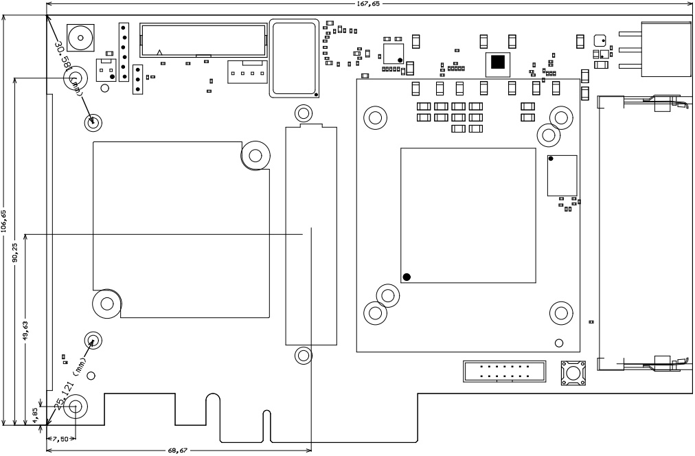
Figure 4: Physical dimensions of the TEC0330-03 board.
Weight
156 g - Plain board.
Revision History
Hardware Revision History
| Date | Revision | Notes | PCN | Documentation |
|---|---|---|---|---|
| - | 03 | First production release | - | - |
| 2015-11-05 | 02 | Prototype | - | - |
| - | 01 | Prototype | - | - |
Table 21: Hardware revision history.
Hardware revision number is printed on the PCB board together with the model number separated by the dash.
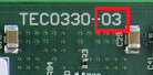
Figure 5: TE0330 board revision number.
Document Change History
| Date | Revision | Contributors | Description |
|---|---|---|---|
| Jan Kumann |
| |
2017-08-30 | v.15 | Jan Kumann |
|
| 2017-03-15 | v.3 | Ali Naseri | Initial TRM release. |
Table 22: Document change history.
Disclaimer
Please also note our data protection declaration at https://www.trenz-electronic.de/en/Data-protection-Privacy The material contained in this document is provided “as is” and is subject to being changed at any time without notice. Trenz Electronic does not warrant the accuracy and completeness of the materials in this document. Further, to the maximum extent permitted by applicable law, Trenz Electronic disclaims all warranties, either express or implied, with regard to this document and any information contained herein, including but not limited to the implied warranties of merchantability, fitness for a particular purpose or non infringement of intellectual property. Trenz Electronic shall not be liable for errors or for incidental or consequential damages in connection with the furnishing, use, or performance of this document or of any information contained herein. In no event will Trenz Electronic, its suppliers, or other third parties mentioned in this document be liable for any damages whatsoever (including, without limitation, those resulting from lost profits, lost data or business interruption) arising out of the use, inability to use, or the results of use of this document, any documents linked to this document, or the materials or information contained at any or all such documents. If your use of the materials or information from this document results in the need for servicing, repair or correction of equipment or data, you assume all costs thereof. No part of this manual may be reproduced in any form or by any means (including electronic storage and retrieval or translation into a foreign language) without prior agreement and written consent from Trenz Electronic. The hardware / firmware / software described in this document are furnished under a license and may be used /modified / copied only in accordance with the terms of such license. To confront directly with the responsibility toward the environment, the global community and eventually also oneself. Such a resolution should be integral part not only of everybody's life. Also enterprises shall be conscious of their social responsibility and contribute to the preservation of our common living space. That is why Trenz Electronic invests in the protection of our Environment. REACH Trenz Electronic is a manufacturer and a distributor of electronic products. It is therefore a so called downstream user in the sense of REACH. The products we supply to you are solely non-chemical products (goods). Moreover and under normal and reasonably foreseeable circumstances of application, the goods supplied to you shall not release any substance. For that, Trenz Electronic is obliged to neither register nor to provide safety data sheet. According to present knowledge and to best of our knowledge, no SVHC (Substances of Very High Concern) on the Candidate List are contained in our products. Furthermore, we will immediately and unsolicited inform our customers in compliance with REACH - Article 33 if any substance present in our goods (above a concentration of 0,1 % weight by weight) will be classified as SVHC by the European Chemicals Agency (ECHA). RoHS Trenz Electronic GmbH herewith declares that all its products are developed, manufactured and distributed RoHS compliant. WEEE Information for users within the European Union in accordance with Directive 2002/96/EC of the European Parliament and of the Council of 27 January 2003 on waste electrical and electronic equipment (WEEE). Users of electrical and electronic equipment in private households are required not to dispose of waste electrical and electronic equipment as unsorted municipal waste and to collect such waste electrical and electronic equipment separately. By the 13 August 2005, Member States shall have ensured that systems are set up allowing final holders and distributors to return waste electrical and electronic equipment at least free of charge. Member States shall ensure the availability and accessibility of the necessary collection facilities. Separate collection is the precondition to ensure specific treatment and recycling of waste electrical and electronic equipment and is necessary to achieve the chosen level of protection of human health and the environment in the European Union. Consumers have to actively contribute to the success of such collection and the return of waste electrical and electronic equipment. Presence of hazardous substances in electrical and electronic equipment results in potential effects on the environment and human health. The symbol consisting of the crossed-out wheeled bin indicates separate collection for waste electrical and electronic equipment. Trenz Electronic is registered under WEEE-Reg.-Nr. DE97922676.Data Privacy
Document Warranty
Limitation of Liability
Copyright Notice
Technology Licenses
Environmental Protection
REACH, RoHS and WEEE
Overview
Content Tools