Table of Contents
Overview
The Trenz Electronic TE0723 is a Arduino compatible FPGA module based on the Xilinx Zynq XC7Z010 SoC.
Key Features
- Xilinx Zynq XC7Z010 SoC
- Dual ARM Cortex A9 processors
- 512 MByte DDR3L SDRAM
- 16 MByte QSPI Flash
- Micro SD Card socket with card detect signal
- ...
Additional assembly options are available for cost or performance optimization upon request.
Block Diagram
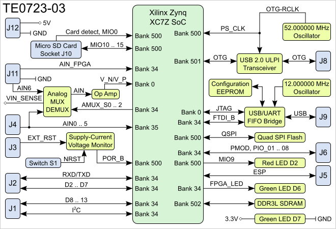
Figure 1: TE0723 block diagram.
Main Components
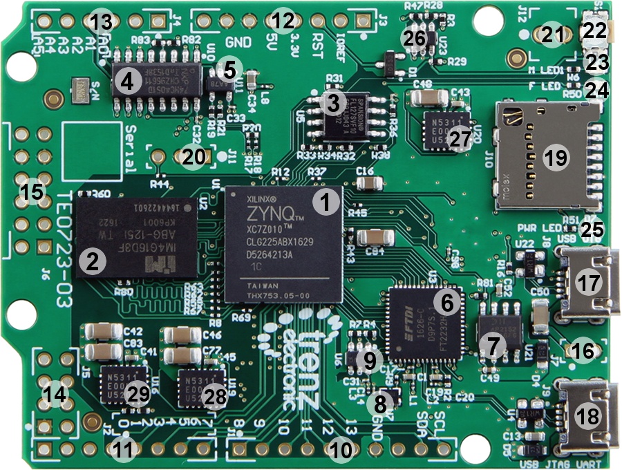
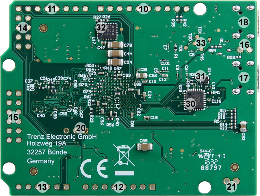
Figure 2: Main components of the TE0723 module.
- Xilinx Zynq XC7Z010 SoC, U1
- 4 Gbit DDR3L 256M x 16 SDRAM, U2
- 16 MByte QSPI Flash memory, U5
High-speed CMOS logic analog multiplexer/demultiplexer, U10
- 1 MHz low-power operational amplifier, U11
- Dual high-speed USB to multipurpose UART/FIFO, U3
- 0.5A dual-channel current-limited power switch, U21
- Low-power programmable oscillator @ 12.000000 MHz, U7
- 2 Kbit Microwire compatible serial EEPROM, U6
- 10-pin header, J1
- 8-pin header, J2
- 10-pin header, J3
- Analog input header, J4
- 2 x 4-pin header, J5
- PMod 2x6 interface header, J6
- USB host mode jumper, J7
- Micro USB 2.0 Type-B receptacle, J8
- Micro USB 2.0 Type-B receptacle, J9
- Micro SD card connector with detect signal, J10
- Analog input select jumper, J11
- 5V supply power input, J12
- Reset switch, S1
- Red LED, D2
- Green LED, D6
- Green LED, D7
- Ultra-low supply-current voltage monitor, U23
1A PowerSoC DC-DC converter (3.3 V), U20
- 1A PowerSoC DC-DC converter (1.8 V, U19
- 1A PowerSoC DC-DC converter (1.35 V), U16
- Hi-speed USB 2.0 ULPI transceiver, U18
- Low-power programmable oscillator @ 52.000000 MHz, U14
- 1A PowerSoC DC-DC converter (1.0 V), U17
- JTAG interface testpoints, TP1-TP4
Initial Delivery State
Storage device name | Content | Notes |
|---|---|---|
Quad SPI Flash | Empty |
Table 1: Initial delivery state of programmable devices on the module.
Boot Process
...
Signals, Interfaces and Pins
I/O Signals
List of I/O signals between PS/PL banks and external connectors:
| Bank | Type | Connector | Signal Count | Voltage | Notes |
|---|---|---|---|---|---|
| 34 | HR | J1 | 6 | 3.3 | D8 .. 13, SDA, SCL |
| 34 | HR | J2 | 8 | 3.3 | D2 .. 7, RXD, TXD |
| 34 | HR | J6 | 8 | 3.3 | PIO01 .. PIO08 |
| 35 | HR | J4 | 7 | 3.3 | AIN0 .. 5 |
| 35 | HR | J5 | 1 | 3.3 | ESP_GPIO2 |
| 500 | MIO | J10 | 6 | 3.3 | SDCARD |
| 501 | MIO | J5 | 4 | 3.3 | ESP_RXD, ESP_TXD, ESP_GPIO0, MOD_RST |
Table x: .
JTAG Interface
JTAG access to the Xilinx Zynq XC7Z010 SoC is provided through testpoints TP1-T4.
JTAG Signal | Testpoint |
|---|---|
| TCK | TP3 |
| TDI | TP1 |
| TDO | TP2 |
| TMS | TP4 |
Table 5: JTAG interface signals.
Default PS MIO Mapping
| MIO | Function | Connected To | Notes |
|---|---|---|---|
| 0 | SDCARD | J10-9 | Card detect switch. |
| 1 | QSPI | U5-1 | SP0-CS |
| 2 | QSPI | U5-5 | SPI0-DQ0 |
| 3 | QSPI | U5-2 | SPI0-DQ1 |
| 4 | QSPI | U5-3 | SPI0-DQ2 |
| 5 | QSPI | U5-7 | SPI0-DQ3 |
| 6 | QSPI | U5-6 | SPI0-SCK |
| 7 | GPIO | U18-27 | USB PHY reset |
| 9 | LED | D2 | Red LED |
| 10 | SDCARD | J10-7 | DAT0 |
| 11 | SDCARD | J10-3 | CMD |
| 12 | SDCARD | J10-5 | CLK |
| 13 | SDCARD | J10-8 | DAT1 |
| 14 | SDCARD | J10-1 | DAT2 |
| 15 | SDCARD | J10-2 | CD/DAT3 |
| 28 | USB-OTG | U18-7 | OTG-DATA4 |
| 29 | USB-OTG | U18-31 | OTG-DIR |
| 30 | USB-OTG | U18-29 | OTG-STP |
| 31 | USB-OTG | U18-2 | OTG-NXT |
| 32 | USB-OTG | U18-3 | OTG-DATA0 |
| 33 | USB-OTG | U18-4 | OTG-DATA1 |
| 34 | USB-OTG | U18-5 | OTG-DATA2 |
| 35 | USB-OTG | U18-6 | OTG-DATA3 |
| 36 | USB-OTG | U18-1 | OTG-CLK |
| 37 | USB-OTG | U18-9 | OTG-DATA5 |
| 38 | USB-OTG | U18-10 | OTG-DATA6 |
| 39 | USB-OTG | U18-13 | OTG-DATA7 |
| 48 | ESP | J5-2 | ESP_TXD |
| 49 | ESP | J5-7 | ESP_RXD |
| 52 | ESP | J5-6 | MOD_RST |
| 53 | ESP | J5-3 | ESP_GPIO0 |
I2C Interface
I2C interface pins from the Zynq SoC PL bank 34 are connected to the connector J1. There are no on-board I2C slave devices.
| Signal | Zynq SoC Pin | Connected To |
|---|---|---|
| SDA | R13 | J1-9 |
| SCL | P13 | J1-10 |
Table x: .
On-board Peripherals
Quad SPI Flash Memory
Clocking
| Clock Signal | Frequency | IC | Signal, Pin |
|---|---|---|---|
Processing system (PS) reference clock. | 52.000000 MHz | U1 | PS_CLK, C7 |
USB transceiver reference clock. | 52.000000 MHz | U18 | OTG-RCLK, 26 |
| High-speed USB to multipurpose UART/FIFO oscillator input. | 12.000000 MHz | U3 | OSCI, 3 |
Table x: .
On-board LEDs
There are three LEDs on-board TE0723:
| LED | Color | Connected To | Description and Notes |
|---|---|---|---|
| D2 | Red | MIO9, U1 | User LED. |
| D6 | Green | U1, bank 34 pin G14 | FPGA_LED |
| D7 | Green | 3.3V | PWR_LED, power-on LED. |
Table x: On-board LEDs.
Power and Power-On Sequence
Power Supply
Single 5V power supply with minimum current capability of 2A for system startup is recommended.
Power Consumption
TBD - To Be Determined.
Power-On Sequence
There is no sequence...
Technical Specifications
Absolute Maximum Ratings
Parameter | Min | Max | Units | Reference Document |
|---|---|---|---|---|
VIN supply voltage | -0.5 | 3.6 | V | Xilinx datasheet DS187, "Zynq-7000 All Programmable SoC: DC and AC Switching Characteristics". |
Storage temperature | -40 | +85 | °C |
Table x: .
Recommended Operating Conditions
| Parameter | Min | Max | Units | Reference Document |
|---|---|---|---|---|
| Supply voltage | 1.14 | 3.465 | V | Xilinx datasheet DS187, "Zynq-7000 All Programmable SoC: DC and AC Switching Characteristics". |
Table x: .
Assembly variants for higher storage temperature range are available on request.
Physical Dimensions
Module size: 68.58 mm × 53.34 mm. Please download the assembly diagram for exact numbers.
PCB thickness: 1.6 mm.
Highest part on PCB: approx. 4 mm. Please download the step model for exact numbers.
Please note that two different units are used on the figures below, SI system millimeters (mm) and imperial system thousandths of an inch(mil). To convert mils to millimeters and vice versa use formula 100mil's = 2,54mm.
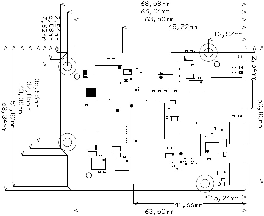
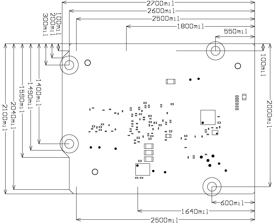
Figure 3: TE0723 module physical dimensions.
Operating Temperature Ranges
Commercial grade: 0°C to +70°C.
Industrial grade: -40°C to +85°C.
Operating temperature range depends also on customer design and cooling solution. Please contact us for options.
Revision History
Hardware Revision History
| Date | Revision | Notes | PCN | Documentation Link |
|---|---|---|---|---|
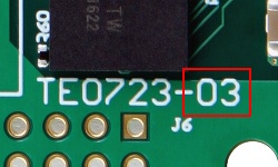
| 2016-07-15 | 03 | Click to see PCN. | TE0723-03 | |
2015-11-06 | 02 | TE0723-02 | ||
01 |
|
Table x: TE0723 hardware revision history.
Hardware revision number is printed on the PCB board together with the module model number separated by the dash.
Document Change History
Date | Revision | Contributors | Description |
|---|---|---|---|
Jan Kumann | Initial document. |
Table x: Document change history.
Disclaimer
Data Privacy
Please also note our data protection declaration at https://www.trenz-electronic.de/en/Data-protection-Privacy
Document Warranty
The material contained in this document is provided “as is” and is subject to being changed at any time without notice. Trenz Electronic does not warrant the accuracy and completeness of the materials in this document. Further, to the maximum extent permitted by applicable law, Trenz Electronic disclaims all warranties, either express or implied, with regard to this document and any information contained herein, including but not limited to the implied warranties of merchantability, fitness for a particular purpose or non infringement of intellectual property. Trenz Electronic shall not be liable for errors or for incidental or consequential damages in connection with the furnishing, use, or performance of this document or of any information contained herein.
Limitation of Liability
In no event will Trenz Electronic, its suppliers, or other third parties mentioned in this document be liable for any damages whatsoever (including, without limitation, those resulting from lost profits, lost data or business interruption) arising out of the use, inability to use, or the results of use of this document, any documents linked to this document, or the materials or information contained at any or all such documents. If your use of the materials or information from this document results in the need for servicing, repair or correction of equipment or data, you assume all costs thereof.
Copyright Notice
No part of this manual may be reproduced in any form or by any means (including electronic storage and retrieval or translation into a foreign language) without prior agreement and written consent from Trenz Electronic.
Technology Licenses
The hardware / firmware / software described in this document are furnished under a license and may be used /modified / copied only in accordance with the terms of such license.
Environmental Protection
To confront directly with the responsibility toward the environment, the global community and eventually also oneself. Such a resolution should be integral part not only of everybody's life. Also enterprises shall be conscious of their social responsibility and contribute to the preservation of our common living space. That is why Trenz Electronic invests in the protection of our Environment.
REACH, RoHS and WEEE
REACH
Trenz Electronic is a manufacturer and a distributor of electronic products. It is therefore a so called downstream user in the sense of REACH. The products we supply to you are solely non-chemical products (goods). Moreover and under normal and reasonably foreseeable circumstances of application, the goods supplied to you shall not release any substance. For that, Trenz Electronic is obliged to neither register nor to provide safety data sheet. According to present knowledge and to best of our knowledge, no SVHC (Substances of Very High Concern) on the Candidate List are contained in our products. Furthermore, we will immediately and unsolicited inform our customers in compliance with REACH - Article 33 if any substance present in our goods (above a concentration of 0,1 % weight by weight) will be classified as SVHC by the European Chemicals Agency (ECHA).
RoHS
Trenz Electronic GmbH herewith declares that all its products are developed, manufactured and distributed RoHS compliant.
WEEE
Information for users within the European Union in accordance with Directive 2002/96/EC of the European Parliament and of the Council of 27 January 2003 on waste electrical and electronic equipment (WEEE).
Users of electrical and electronic equipment in private households are required not to dispose of waste electrical and electronic equipment as unsorted municipal waste and to collect such waste electrical and electronic equipment separately. By the 13 August 2005, Member States shall have ensured that systems are set up allowing final holders and distributors to return waste electrical and electronic equipment at least free of charge. Member States shall ensure the availability and accessibility of the necessary collection facilities. Separate collection is the precondition to ensure specific treatment and recycling of waste electrical and electronic equipment and is necessary to achieve the chosen level of protection of human health and the environment in the European Union. Consumers have to actively contribute to the success of such collection and the return of waste electrical and electronic equipment. Presence of hazardous substances in electrical and electronic equipment results in potential effects on the environment and human health. The symbol consisting of the crossed-out wheeled bin indicates separate collection for waste electrical and electronic equipment.
Trenz Electronic is registered under WEEE-Reg.-Nr. DE97922676.
Overview
Content Tools