Table of Contents
Overview
The Trenz Electronic TE0714 is an industrial-grade SoM (System on Module) based on Xilinx Artix-7, 16 MByte Flash memory and powerful switching mode power supplies for all on-board voltages. A large number of configurable I/O's is provided via rugged high-speed stacking strips. TE0714 is the smallest module with transceiver (3 x 4 cm).
Key Features
Xilinx Artix-7 FPGA (A15T, A35T, A50T)
- Rugged for shock and high vibration
- 16 MByte QSPI Flash memory
- Differential MEMS oscillator for MGT clocking
- MEMS oscillator for PL clocks (Optional)
- Plug-on module with 2 × 100-pin high-speed hermaphroditic strips
- 144 FPGA I/O's (Max 68 differential)
- XADC analog input
- 4 GTP (high-performance transceiver) lanes
- GT reference clock inputs
- Optimized I/O and power pins for good signal integrity
- On-board high-efficiency DC-DC converters
- Power supply for all on-board components
- eFUSE bit-stream encryption (AES)
- One user configurable LED
Different configurations for cost and performance optimization available upon request. Available options are:
- FPGA Type (A15T, A35T, A50T), temperature grade
- GT clock frequency (or none if not implemented)
- PL clock frequency and precision (or none if not implemented)
- Config and B14 bank Voltage: 1.8V or 3.3V
- SPI Flash type (or none if not implemented)
- LED Color (or none if not implemented)
- PUDC Pin strapping (pull high or pull down)
- GT power enable pin strapping (default power enabled or disabled)
Block Diagram
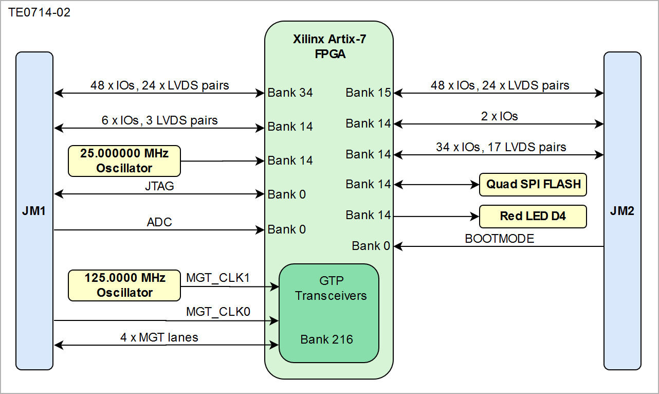
Main Components
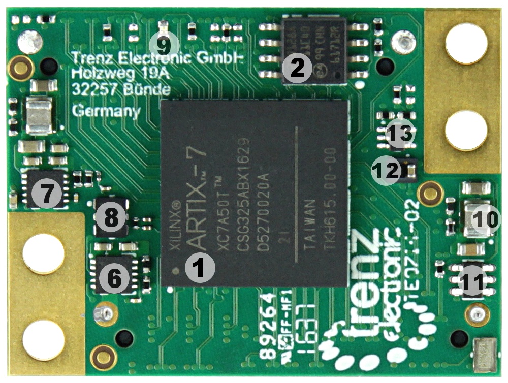
- Xilinx Artix-7 FPGA (XC7A series), U4
- 16 MByte SPI Flash, U7
- B2B connector Samtec Razor Beam™ LSHM-150, JM2
- B2B connector Samtec Razor Beam™ LSHM-150, JM1
- 25 MHz oscillator, U8
- Single output low-dropout linear regulator (1.2V_MGT), U6
- Single output low-dropout linear regulator (1.0V_MGT), U5
- Low-jitter precision LVDS 125 MHz oscillator (GT Clock), U2
- Red indication LED, D4
- Step-down DC-DC converter (1.0V), U1
- PFET load switch with configurable slew rate (3.3V), Q1
- Low-power step-down DC-DC converter (1.8V), U3
- Voltage detector for circuit initialization and timing supervision, U23
Initial Delivery State
Storage device name | Content | Notes |
|---|---|---|
SPI Flash OTP Area | Empty, not programmed | Except serial number programmed by flash vendor |
SPI Flash Quad Enable bit | Programmed | |
SPI Flash main array | demo design | |
eFUSE USER | Not programmed | |
eFUSE Security | Not programmed |
Signals, Interfaces and Pins
Board to Board (B2B) I/Os
FPGA bank number and number of I/O signals connected to the B2B connector:
| FPGA Bank | B2B Connector | I/O Signal Count | Voltage Level | Notes |
|---|---|---|---|---|
| 14 | JM1 | 6 | VCCIO_0 | |
| 14 | JM2 | 36 | VCCIO_0 | NB! 17 LVDS pairs possible. |
| 15 | JM2 | 48 | VCCIO15 | Supplied by the baseboard. |
| 34 | JM1 | 48 | VCCIO34 | Supplied by the baseboard. |
| 216 | JM1 | 16 | MGT_AVCC MGT_AVTT | 4 x GTP lanes. |
Please refer to the Pin-out tables page for additional information.
JTAG Interface
JTAG access to the Xilinx Artix-7 FPGA device is provided through connector JM1.
Signal Name | B2B Pin |
|---|---|
| TCK | JM1:89 |
| TDI | JM1:85 |
| TDO | JM1:87 |
| TMS | JM1:91 |
On-board LED's
There is one LED on TE0714 module:
LED | Color | FPGA | Notes |
|---|---|---|---|
D4 | Red | K18 |
|
Clocking
Clock | Default Frequency | IC | FPGA | Notes |
|---|---|---|---|---|
| CLK125MHz | 25 MHz | U8 | T14 | Frequency depends on the module variant. Output is compatible to 3.3V and 1.8V I/O standard of the FPGA bank. |
| MGT_CLK | 125MHz | U2 | B6/B5 | Frequency depends on the module variant |
Boot Process
Boot mode is controlled by the MODE signal on the board to board (B2B) connector:
MODE signal State | Boot Mode |
|---|---|
high or open | Master SPI, x4 Mode |
low or ground | Slave SelectMAP |
SPI D2 and D3 have no pull-ups on the module so with PUDC=High option, those pins are floating if there are no pull-ups on baseboard. As those pins have SPI RESET function when Quad mode is not enabled, it is mandatory to either add pull-ups on user baseboard or program the Quad Enable bit in Flash nonvolatile status register.
On-board Peripherals
16 MByte Quad SPI Flash
On-board SPI flash memory S25FL127S (U7) is used to store initial FPGA configuration. Besides FPGA configuration, remaining free flash memory can be used for user application storage. All four SPI data lines are connected to the FPGA allowing x1, x2 or x4 data bus widths. Maximum data rate depends on the bus width and clock frequency used.
SPI Flash QE (Quad Enable) bit must be set to high or FPGA is unable to load its configuration from flash. By default this bit is set to high at the manufacturing plant.
Power and Power-On Sequence
To power-up a module, power supply with minimum current capability of 1A is recommended.
Power Supply
TE0714 needs one single power supply with nominal of 3.3V.
Power Consumption
| Test Condition (25 °C ambient) | VIN Current mA | Notes |
|---|---|---|
| TE0714-35, TEBT0714, empty design, GT not enabled | 110mA |
Actual power consumption depends on the FPGA design and ambient temperature.
Power-On Sequence
There is no specific or special power-on sequence, single power source is needed as VIN, rest of the sequence is automatic.
Bank Voltages
Bank | Voltage | Notes |
|---|---|---|
0 Config and B14 | 1.8V or 3.3V | Depends on module variant |
15 | User | Supplied from baseboard via B2B connector, max 3.3V |
34 | User | Supplied from baseboard via B2B connector, max 3.3V |
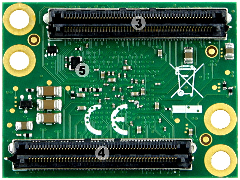
Board to Board Connectors
Board to board connectors are hermaphroditic. Odd pin numbers are connected to even pin numbers on the mating connector and vice versa.
The Trenz Electronic modules use 100-pin REF-189016-02 and 60-pin REF-189017-02 connectors which are compatible with Samtec Razor Beam LSHM type connectors (see table below). When using the same type of connectors on baseboard, mating height will be 8mm. Other mating heights are possible by using connectors with a different height.
| Baseboard Connector | Compatible Connector | Number of Pins | Mating height |
|---|---|---|---|
| REF-189016-01 | LSHM-150-02.5-L-DV-A-S-K-TR | 100 (2 x 50) | 6.5 mm |
| LSHM-150-03.0-L-DV-A-S-K-TR | LSHM-150-03.0-L-DV-A-S-K-TR | 100 (2 x 50) | 7.0 mm |
| REF-189016-02 | LSHM-150-04.0-L-DV-A-S-K-TR | 100 (2 x 50) | 8.0 mm |
| LSHM-150-06.0-L-DV-A-S-K-TR | LSHM-150-06.0-L-DV-A-S-K-TR | 100 (2 x 50) | 10.0mm |
| REF-189017-01 | LSHM-130-02.5-L-DV-A-S-K-TR | 60 (2 x 30) | 6.5 mm |
| LSHM-130-03.0-L-DV-A-S-K-TR | LSHM-130-03.0-L-DV-A-S-K-TR | 60 (2 x 30) | 7.0 mm |
| REF-189017-02 | LSHM-130-04.0-L-DV-A-S-K-TR | 60 (2 x 30) | 8.0 mm |
| LSHM-130-06.0-L-DV-A-S-K-TR | LSHM-130-06.0-L-DV-A-S-K-TR | 60 (2 x 30) | 10.0mm |
Modules can be manufactured using different type of connectors upon request.
The LSHM connector speed rating depends on the stacking height:
| Stacking Height | Speed Rating |
|---|---|
| 12 mm, Single-Ended | 7.5 GHz / 15 Gbps |
| 12 mm, Differential | 6.5 GHz / 13 Gbps |
| 5 mm, Single-Ended | 11.5 GHz / 23 Gbps |
| 5 mm, Differential | 7.9 GHz / 14 Gbps |
Connector Mechanical Ratings
- Shock: 100G, 6 ms Sine
- Vibration: 7.5G random, 3 hours 3 axis
Manufacturer Documentation
Variants Currently In Production
| Module Variant | FPGA Chip Model | B14/Config Voltage [V] | R27 (VCCIO_0 on JM2 Pin 54) | SPI Flash |
|---|---|---|---|---|
| TE0714-02-35-2I | XC7A35T-2CSG325I | 3.3 | JM2 Pin 54 = VCCIO_0 (3.3 V) | S25FL127S |
| TE0714-02-35-2IC6 | XC7A35T-2CSG325I | 1.8 | JM2 Pin 54 = Open | N25Q128 |
| TE0714-02-50-2I | XC7A50T-2CSG325I | 3.3 | JM2 Pin 54 = VCCIO_0 (3.3 V) | S25FL127S |
| TE0714-02-50-2IC6 | XC7A50T-2CSG325I | 1.8 | JM2 Pin 54 = Open | N25Q128 |
On REV 01 JM2 Pin 54 was connected to GND. When R27 is not populated, REV 02 is backwards compatible to REV 01. When R27 is set, check your baseboard to not connect this pin to GND. For all new baseboards JM2.54 should be used as VCCIO output (it will then be 1.8V or 3.3V depending the voltage settings on the module.
Technical Specifications
Absolute Maximum Ratings
Parameter | Min | Max | Units | Notes |
|---|---|---|---|---|
VIN supply voltage | -0.1 | 6.0 | V | - |
| HR I/O banks supply voltage (VCCO) | -0.5 | 3.6 | V | Xilinx datasheet DS181 |
| HR I/O banks input voltage | -0.4 | VCCO + 0.55 | V | Xilinx datasheet DS181 |
| GTP transceivers Tx/Rx input voltage | -0.5 | 1.26 | V | Xilinx datasheet DS181 |
Voltage on module JTAG pins | -0.4 | VCCO_0 + 0.55 | V | Xilinx datasheet DS181 |
Storage temperature | -40 | +85 | °C | - |
Recommended Operating Conditions
| Parameter | Min | Max | Units | Notes |
|---|---|---|---|---|
| VIN supply voltage | 3.135 | 3.45 | V | - |
| HR I/O banks supply voltage (VCCO) | 1.14 | 3.465 | V | Xilinx datasheet DS181 |
| HR I/O banks input voltage | -0.20 | VCCO + 0.20 | V | Xilinx datasheet DS181 |
| Voltage on module JTAG pins | 3.135 | 3.465 | V | Xilinx datasheet DS181 |
Operating Temperature Ranges
Commercial grade: 0°C to +70°C.
Industrial grade: -40°C to +85°C.
Operating temperature range depends also on customer design and cooling solution. Please contact us for options.
Please check Xilinx datasheet DS181 for complete list of absolute maximum and recommended operating ratings for the Artix-7.
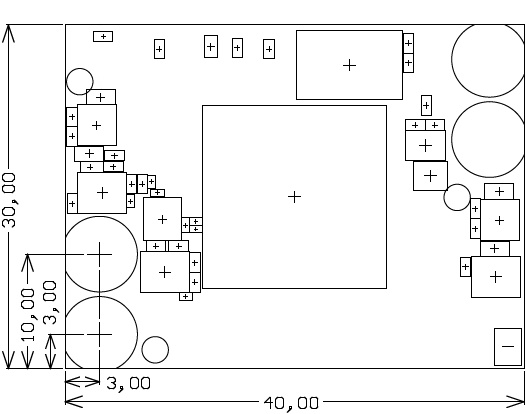
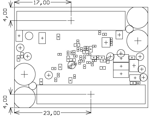
Physical Dimensions
Module size: 40 mm × 30 mm. Please download the assembly diagram for exact numbers.
Mating height with standard connectors: 8 mm
PCB thickness: 1.6 mm
Highest part on PCB: approximately 2.5 mm. Please download the step model for exact numbers.
All dimensions are shown in mm. Additional sketches, drawings and schematics can be found here.
Weight
| Variant | Weight in g | Note |
|---|---|---|
| 2IC6 | 8.3 | Plain Module |
Revision History
Hardware Revision History
| Date | Revision | Notes | PCN Link | Documentation Link |
|---|---|---|---|---|
| 2016-08-04 | 02 | VCCIO0 added to B2B | PCN-20160815 | TE0714-02 |
01 | - | - | TE0714-01 |
Hardware revision number is printed on the PCB board next to the module model number separated by the dash.
Document Change History
Date | Revision | Authors | Description |
|---|---|---|---|
| 2017-05-28 | Jan Kumann | Board-to-Board I/O section added. New physical dimensions images. Documents sections rearranged. | |
| 2017-03-20 | V.26 | John Hartfiel | Notes on Clocking section. |
| 2017-01-27 | v.25 | Jan Kumann | New block diagram. |
| 2016-12-01 | v.17 | Jan Kumann | Changes in the document structure, few corrections. |
| 2016-11-18 | v.14 | Thorsten Trenz, Emmanuel Vassilakis | Hardware revision 02 specific changes. |
2016-06-01 | v.9 | Antti Lukats | Initial version. |
Disclaimer
Data Privacy
Please also note our data protection declaration at https://www.trenz-electronic.de/en/Data-protection-Privacy
Document Warranty
The material contained in this document is provided “as is” and is subject to being changed at any time without notice. Trenz Electronic does not warrant the accuracy and completeness of the materials in this document. Further, to the maximum extent permitted by applicable law, Trenz Electronic disclaims all warranties, either express or implied, with regard to this document and any information contained herein, including but not limited to the implied warranties of merchantability, fitness for a particular purpose or non infringement of intellectual property. Trenz Electronic shall not be liable for errors or for incidental or consequential damages in connection with the furnishing, use, or performance of this document or of any information contained herein.
Limitation of Liability
In no event will Trenz Electronic, its suppliers, or other third parties mentioned in this document be liable for any damages whatsoever (including, without limitation, those resulting from lost profits, lost data or business interruption) arising out of the use, inability to use, or the results of use of this document, any documents linked to this document, or the materials or information contained at any or all such documents. If your use of the materials or information from this document results in the need for servicing, repair or correction of equipment or data, you assume all costs thereof.
Copyright Notice
No part of this manual may be reproduced in any form or by any means (including electronic storage and retrieval or translation into a foreign language) without prior agreement and written consent from Trenz Electronic.
Technology Licenses
The hardware / firmware / software described in this document are furnished under a license and may be used /modified / copied only in accordance with the terms of such license.
Environmental Protection
To confront directly with the responsibility toward the environment, the global community and eventually also oneself. Such a resolution should be integral part not only of everybody's life. Also enterprises shall be conscious of their social responsibility and contribute to the preservation of our common living space. That is why Trenz Electronic invests in the protection of our Environment.
REACH, RoHS and WEEE
REACH
Trenz Electronic is a manufacturer and a distributor of electronic products. It is therefore a so called downstream user in the sense of REACH. The products we supply to you are solely non-chemical products (goods). Moreover and under normal and reasonably foreseeable circumstances of application, the goods supplied to you shall not release any substance. For that, Trenz Electronic is obliged to neither register nor to provide safety data sheet. According to present knowledge and to best of our knowledge, no SVHC (Substances of Very High Concern) on the Candidate List are contained in our products. Furthermore, we will immediately and unsolicited inform our customers in compliance with REACH - Article 33 if any substance present in our goods (above a concentration of 0,1 % weight by weight) will be classified as SVHC by the European Chemicals Agency (ECHA).
RoHS
Trenz Electronic GmbH herewith declares that all its products are developed, manufactured and distributed RoHS compliant.
WEEE
Information for users within the European Union in accordance with Directive 2002/96/EC of the European Parliament and of the Council of 27 January 2003 on waste electrical and electronic equipment (WEEE).
Users of electrical and electronic equipment in private households are required not to dispose of waste electrical and electronic equipment as unsorted municipal waste and to collect such waste electrical and electronic equipment separately. By the 13 August 2005, Member States shall have ensured that systems are set up allowing final holders and distributors to return waste electrical and electronic equipment at least free of charge. Member States shall ensure the availability and accessibility of the necessary collection facilities. Separate collection is the precondition to ensure specific treatment and recycling of waste electrical and electronic equipment and is necessary to achieve the chosen level of protection of human health and the environment in the European Union. Consumers have to actively contribute to the success of such collection and the return of waste electrical and electronic equipment. Presence of hazardous substances in electrical and electronic equipment results in potential effects on the environment and human health. The symbol consisting of the crossed-out wheeled bin indicates separate collection for waste electrical and electronic equipment.
Trenz Electronic is registered under WEEE-Reg.-Nr. DE97922676.
Refer to https://wiki.trenz-electronic.de/display/PD/TE0713+TRM for online version of this manual and the rest of available documentation.
Overview
Content Tools