Table of Contents
Overview
The Trenz Electronic TEF0008 is a FPGA to Mezzanine Card (FMC) based on VITA 57.1 FMC HPC Standard, with four SFP+ 10Gb ports for fiber optical SFP modules. It is inteded for use on a FMC HPC carrier and can not be used stand-alone.
Key Features
- Four SFP+ 10Gb ports
- HPC FMC connector
- Low jitter programmable clock generator
- Intel(Altera) Max10 FPGA 10M08SAU169C8G
- Status LED (green)
Block Diagram
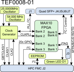
Figure 1: TEF0008-01 block diagram.
Main Components
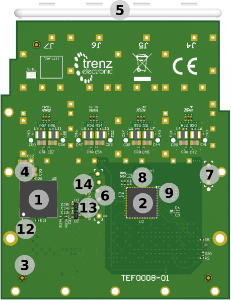
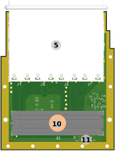
Figure 2: TEF0008-01 FMC overview.
Table 1: TEF0008-01 main components.
- MAX10 FPGA, U5
- Programmable low jitter clock generator Si5354A, U2
- Status LED (green), D1
- 3.3V to 1.8V DCDC converter, U6
- Quad SFP+ cage and connectors, J4-J7
- 1x6 pin header for JTAG programming of FPGA (3.3V), J3
- 1x3 pin header for I²C (1.8V), J1
- XTAL 54.0000 MHz (CX3225SB), Y1
- Oszillator 25.000000 MHz (SiT8008B), U1
- HPC FMC connector, J2
- 128KBit EEPROM, U4
- Testpoints Max10, TP7-TP9
- Testpoints JTAG, TP1-TP4
- Testpoints Power, TP5, TP6, TP10
Initial Delivery State
Storage device name | Content | Notes |
|---|---|---|
Max10 FPGA 10M08SAU169C8G | Programmed | U5. Level shifter and controlller functions. |
Clock generator Si5345A-B-GM | Programmed | U2. OUT0 25MHz, OUT2 125MHz, OUT7 156.25 MHz, OUT8 156.25MHz, OUT9 125MHz. |
EEPROM 24LC128-I/ST | empty | U4, IPMI and VITA57.1 compatible. |
Table 2: Initial delivery state of programmable devices on the module.
Boot Process
The MAX10 FPGA boots form its internal configuration flash memory, which is programmable via JTAG (J3).
Signals, Interfaces and Pins
Board to Board (B2B) I/Os
I/O signals connected to the FPGA I/O bank and B2B connector:
| Bank | Type | B2B Connector | I/O Signal Count | Bank Voltage | Notes |
|---|---|---|---|---|---|
| 3 | GPI/Os | J2 | 20 I/Os | VADJ | Supplied by the carrier board. |
Table 3: General overview of I/O signals connected to the B2B connectors.
MGT Lanes
MGT (Multi Gigabit Transceiver) lane consists of one transmit and one receive (TD/RD) differential pairs, two signals each or four signals total per one MGT lane. Following table lists lane number, MGT bank number, transceiver type, signal schematic name, and HPC FMC Pin:
| Lane | SFP+ | Signal Name | HPC FMC Pin |
|---|---|---|---|
| 0 | J4 |
|
|
| 1 | J5 |
|
|
| 2 | J6 |
|
|
| 3 | J7 |
|
|
Table 4: MGT lanes.
Below are listed MGT banks reference clock sources.
| Clock signal | Source | HPC FMC Pin | Notes |
|---|---|---|---|
| GBTCLK0_P | U2-51 | J2-D4, GBTCLK0_M2C_P | On-board Si5345A. |
| GBTCLK0_N | U2-50 | J2-D5, GBTCLK0_M2C_N | On-board Si5345A. |
| GBTCLK1_P | U2-31 | J2-B20, GBTCLK1_M2C_P | On-board Si5345A. |
| GBTCLK1_N | U2-30 | J2-B21, GBTCLK1_M2C_N | On-board Si5345A. |
Table 5: MGT reference clock sources.
SFP+ Control Interface
Follwowing table contains a brief description of the control and status signals of the SFP+ connectors:
| Signal Schematic Name | FPGA Direction | Description | Logic |
|---|---|---|---|
| SFPx_TX_DISABLE | Output | SFP Enabled / Disabled | Low active |
| SFPx_LOS | Input | Loss of receiver signal | High active |
| SFPx_RS0 | Output | Full RX bandwidth | Low active |
| SFPx_RS1 | Output | Reduced RX bandwidth | Low active |
| SFPx_M-DEF0 | Input | Module present / not present | Low active |
| SFPx_TX_FAULT | Input | Fault / Normal Operation | High active |
| SFPx_SDA | BiDir | 2-wire Serial Interface Data | - |
| SFPx_SCL | Output (BiDir) | 2-wire Serial Interface Clock | - |
Up to 100kHz the modules operate without clock streching. Therfore SCL can be implemented as driven by Master only.
JTAG Interface
JTAG access to the MAX10 FPGA is provided through HPC FMC Connector and an additional pin header connector as well as testpoints.
JTAG Signal | HPC FMC Pin | Pin Header | Testpoints |
|---|---|---|---|
| TCK | J2-D29 | J3-4 | TP2 |
| TDI | J2-D33 | J3-2 | TP1 |
| TDO | J2-D30 | J3-3 | TP3 |
| TMS | J2-D31 | J3-1 | TP4 |
Table 6: JTAG interface signals.
I2C Interface
On-board I2C devices are connected to the MAX10 FPGA for level shift and I²C MUX. Addresses for on-board devices are listed in the table below:
| I2C Device | I2C Address | Notes |
|---|---|---|
| J4, SFP+ | 1100001 / 1100000 | Conventional SFP Memory / Enhanced Feature Set Memory, Device select via MAX10 FPGA implementation. |
| J5, SFP+ | 1100001 / 1100000 | Conventional SFP Memory / Enhanced Feature Set Memory, Device select via MAX10 FPGA implementation. |
| J6, SFP+ | 1100001 / 1100000 | Conventional SFP Memory / Enhanced Feature Set Memory, Device select via MAX10 FPGA implementation. |
| J7, SFP+ | 1100001 / 1100000 | Conventional SFP Memory / Enhanced Feature Set Memory, Device select via MAX10 FPGA implementation. |
| U2, Si5345A | 1101001 | Level shifted via MAX10 FPGA, Device select via MAX10 FPGA implementation. |
| U4, EEPROM | 10100xx | Last digits determined by carrier board via HPC FMC (C34 GA0, C35 GA1).1 |
Table 7: I2C slave device addresses.
1EEPROM FMC SDA and SCL are routed to the FPGA, but this will be removed in future releases due to incompatible power requirments. (VAUX is not a suitable FPGA Bank supply, currently it is routed to a Bank with conflicting VADJ supply).
On-board Peripherals
Programmable Clock Generator
There is a Silicon Labs I2C programmable clock generator on-board (Si5345A, U2) to generate reference clocks for the module. Programming can be done using I2C via PIN header J1. The I2C bus is also routed to the MAX10 FPGA.
| Si5345A Pin | Signal Name / Description | Connected To | Direction | Note |
|---|---|---|---|---|
IN0 | Reference input clock. | U1 | Input | 25.000000 MHz oscillator, Si8208AI |
| IN1 | - | Not connected. | Input | Not used. |
IN2 | - | Not connected. | Input | Not used. |
IN3 | CLK2 | J2-K4/K5 | Input | HPC FMC configured as C2M clock. |
A1 | - | GND | Input | I2C slave device address LSB. |
| XAXB | - | Y1 | Input | 54.0000 MHz XTAL CX3225SB |
OUT0 | CLKPLL2F | U5-H6/G5 | Output | FPGA bank 2. |
| OUT1 | - | Not connected. | Output | Not used. |
| OUT2 | GBTCLK1 | J2-B20/B21 | Output | M2C via HPC FMC. |
| OUT3 | - | Not connected. | Output | Not used. |
| OUT4 | - | Not connected. | Output | Not used. |
| OUT5 | - | Not connected. | Output | Not used. |
| OUT6 | - | Not connected. | Output | Not used. |
| OUT7 | GBTCLK0 | J2-D4/D5 | Output | M2C via HPC FMC. |
| OUT8 | CLK0 | J2-H4/H5 | Output | M2C via HPC FMC. |
| OUT9 | CLK1 | J2-G2/G3 | Output | M2C via HPC FMC. |
Table 8: Programmable clock generator inputs and outputs.
Oscillators
The module has following reference clock signals provided by on-board oscillators and external source from carrier board:
| Clock Source | Schematic Name | Frequency | Clock Destination |
|---|---|---|---|
| SiTime SiT8008AI oscillator, U1 | - | 25.000000 MHz | U2-63/64 |
| Carrier board via HPC FMC J2-K4/K5 | CLK2 | Defined by carrier. | U2-61/62 |
Table 9: Reference clock signals.
EEPROM
A Microchip 24LC128-I/LC serial EEPROM (U4) is provided for IPMI data. It is acceasible via the LPC FMC connector (SCL C30, SDA C31).
On-board LED
| LED | Color | Connected to | Description and Notes |
|---|---|---|---|
| D1 | Green | U5-C2 (bank 1A) | Depending on FPGA design. With the shiped FPGA design it is on if at least on SFP is connected. |
Table 10: On-board LED.
Power and Power-On Sequence
Power Consumption
The maximum power consumption of a module depends on the design running on the FPGA.
| 3P3V | TBD* |
| VADJ (at 1.8V) | TBD* |
3P3VAUX | TBD* |
Table 11: Typical power consumption.
* TBD - To Be Determined with reference design setup.
Power Distribution Dependencies
Regulator dependencies and max. current.
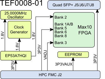
Figure 3: Module power distribution diagram.
Power Rails
Power Rail Name | HPC FMC Connector (J2) | Direction | Notes |
|---|---|---|---|
| 3P3V | D36, D38, D40, C39 | Input | Supply voltage from carrier board. |
| 1.8V | - | Output | Module on-board 1.8V voltage supply (Max 1A). |
| 3P3VAUX | D32 | Input | Supply voltage from carrier board. |
VADJ | H40, G39, F40, E39 | Input | Supply voltage from carrier board. |
| 12V | C35, C37 | Input | Not used supply voltage from carrier board. |
Table 12: Module power rails.
Bank Voltages
Bank | Schematic Name | Voltage | Voltage Range |
|---|---|---|---|
| 1A | 3P3V | 3.3V | - |
| 1B | 3P3V | 3.3V | - |
| 2 | 1.8V | 1.8V | - |
| 3 | VADJ | Carrier supplied | 1.2V - 3.3V |
| 5 | 3P3V | 3.3V | - |
| 6 | 3P3V | 3.3V | - |
| 8 | 3P3V | 3.3V | - |
Table 13: Module PL I/O bank voltages.
Variants Currently In Production
| Module Variant | FPGA | Operating Temperature | Temperature Range |
|---|---|---|---|
| TE0008-01 | 10M08SAU169C8G | 0°C to +85°C | Commercial |
Table 14: Module variants.
Technical Specifications
Absolute Maximum Ratings
Parameter | Min | Max | Units | Reference Document |
|---|---|---|---|---|
Storage temperature | -40 | 85 | °C | - |
Table 15: Module absolute maximum ratings.
Operating Temperature Ranges
Commercial grade: 0°C to +70°C.
Physical Dimensions
Module size: 69 mm × 84 mm, SFP+ conector excluded (+ 5.5 mm). See Vita 57.1 standard.
PCB thickness: 1.6 mm.
Highest part on PCB top is 9.5 mm (SFP+ cage, excluded front plate), bottom 1.4 mm (MAX10 FPGA). Please download the step model for exact numbers.
All dimensions are given in millimeters.
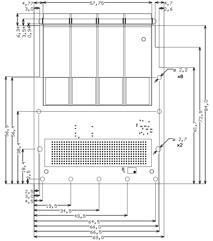
Figure 4: Module physical dimensions drawing
Mounting holes near the front pannel are not implemented due to physical restrictions caused by the SFP cage. The dimensions exceed in some area the by Vita 57.1 standard defined dimensions. In the middle region of the card the cage is higher than the specified max high for this area. Check carefully if the carrier card uses this space for other components conflicting mechanical. The bottom side is at the high limit.
Revision History
Hardware Revision History
| Date | Revision | Notes | PCN | Documentation Link |
|---|---|---|---|---|
| - | 01 |
Table 17: Module hardware revision history.
Hardware revision number can be found on the PCB board together with the module model number separated by the dash.
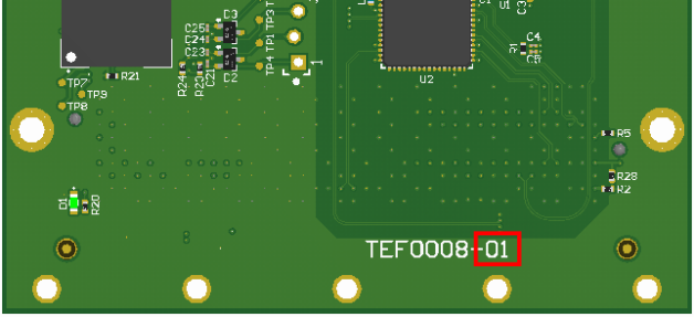
Figure 5: Module hardware revision number.
Document Change History
Date | Revision | Contributors | Description |
|---|---|---|---|
| Author Name | What changed? | ||
2018-05-30 | Martin Rohrmüller | Initial document. | |
all | Jan Kumann, John Hartfiel |
Table 18: Document change history.
Disclaimer
Data Privacy
Please also note our data protection declaration at https://www.trenz-electronic.de/en/Data-protection-Privacy
Document Warranty
The material contained in this document is provided “as is” and is subject to being changed at any time without notice. Trenz Electronic does not warrant the accuracy and completeness of the materials in this document. Further, to the maximum extent permitted by applicable law, Trenz Electronic disclaims all warranties, either express or implied, with regard to this document and any information contained herein, including but not limited to the implied warranties of merchantability, fitness for a particular purpose or non infringement of intellectual property. Trenz Electronic shall not be liable for errors or for incidental or consequential damages in connection with the furnishing, use, or performance of this document or of any information contained herein.
Limitation of Liability
In no event will Trenz Electronic, its suppliers, or other third parties mentioned in this document be liable for any damages whatsoever (including, without limitation, those resulting from lost profits, lost data or business interruption) arising out of the use, inability to use, or the results of use of this document, any documents linked to this document, or the materials or information contained at any or all such documents. If your use of the materials or information from this document results in the need for servicing, repair or correction of equipment or data, you assume all costs thereof.
Copyright Notice
No part of this manual may be reproduced in any form or by any means (including electronic storage and retrieval or translation into a foreign language) without prior agreement and written consent from Trenz Electronic.
Technology Licenses
The hardware / firmware / software described in this document are furnished under a license and may be used /modified / copied only in accordance with the terms of such license.
Environmental Protection
To confront directly with the responsibility toward the environment, the global community and eventually also oneself. Such a resolution should be integral part not only of everybody's life. Also enterprises shall be conscious of their social responsibility and contribute to the preservation of our common living space. That is why Trenz Electronic invests in the protection of our Environment.
REACH, RoHS and WEEE
REACH
Trenz Electronic is a manufacturer and a distributor of electronic products. It is therefore a so called downstream user in the sense of REACH. The products we supply to you are solely non-chemical products (goods). Moreover and under normal and reasonably foreseeable circumstances of application, the goods supplied to you shall not release any substance. For that, Trenz Electronic is obliged to neither register nor to provide safety data sheet. According to present knowledge and to best of our knowledge, no SVHC (Substances of Very High Concern) on the Candidate List are contained in our products. Furthermore, we will immediately and unsolicited inform our customers in compliance with REACH - Article 33 if any substance present in our goods (above a concentration of 0,1 % weight by weight) will be classified as SVHC by the European Chemicals Agency (ECHA).
RoHS
Trenz Electronic GmbH herewith declares that all its products are developed, manufactured and distributed RoHS compliant.
WEEE
Information for users within the European Union in accordance with Directive 2002/96/EC of the European Parliament and of the Council of 27 January 2003 on waste electrical and electronic equipment (WEEE).
Users of electrical and electronic equipment in private households are required not to dispose of waste electrical and electronic equipment as unsorted municipal waste and to collect such waste electrical and electronic equipment separately. By the 13 August 2005, Member States shall have ensured that systems are set up allowing final holders and distributors to return waste electrical and electronic equipment at least free of charge. Member States shall ensure the availability and accessibility of the necessary collection facilities. Separate collection is the precondition to ensure specific treatment and recycling of waste electrical and electronic equipment and is necessary to achieve the chosen level of protection of human health and the environment in the European Union. Consumers have to actively contribute to the success of such collection and the return of waste electrical and electronic equipment. Presence of hazardous substances in electrical and electronic equipment results in potential effects on the environment and human health. The symbol consisting of the crossed-out wheeled bin indicates separate collection for waste electrical and electronic equipment.
Trenz Electronic is registered under WEEE-Reg.-Nr. DE97922676.
Overview
Content Tools