Overview
Firmware for PCB CPLD with designator U26 : LCMX02-256HC
Feature Summary
- Power Management
- Reset
- CPLD JTAG
- Boot Mode
- PUDC
- ETH
- LED
- I2C
Firmware Revision and supported PCB Revision
See Document Change History
Product Specification
Port Description
| Name / opt. VHD Name | Direction | Pin | Pullup/Down | Bank Power | Description |
|---|---|---|---|---|---|
| LED / LED | OUT | 25 | NONE | 3.3VIN | Red LED D3 |
| CONFIG | OUT | 4 | NONE | 1.8V | ETH config pin |
| EN1 / EN1 | IN | 32 | UP | 3.3VIN | B2B Power Enable - Old name from PCB REV04 and earlier : EN1 / EN_SC3 |
| JTAGEN / --- | IN | 26 | --- | 3.3VIN | JTAG enable for CPLD Firmware update |
| MODE /MODE | IN | 30 | UP | 3.3VIN | B2B Boot Mode Pin- Old name from PCB REV04 and earlier : MODE /MODE_SC1 |
| MODE0_R / MODE0_R | OUT | 12 | NONE | 3.3V | Zynq Boot Mode Pin- Old name from PCB REV04 and earlier : MODE0_R / BOOT_R0 |
| MODE2_R / MODE2_R | OUT | 17 | NONE | 3.3V | Zynq Boot Mode Pin- Old name from PCB REV04 and earlier : MODE2_R / BOOT_R2 |
| MODE3_R / MODE3_R | OUT | 13 | NONE | 3.3V | Zynq Boot Mode Pin- Old name from PCB REV04 and earlier : MODE3_R / BOOT_R3 |
| MR / MR | OUT | 10 | UP | 3.3V | Zynq Reset - Old name from PCB REV04 and earlier : MR / POR_B |
| SPI_SCK_FB/VCFG1 | OUT | 8 | NONE | 3.3V | Only for PCB REV05 and later. This pin is connected to MIO8 to change Bank 1 voltage for some applications like boundary scan to test MIOs. |
| RST / --- | --- | 9 | --- | 3.3V | / currently_not_used |
| NOSEQ / NOSEQ | INOUT | 29 | UP | 3.3VIN | NOSEQ pin- Old name from PCB REV04 and earlier : NOSEQ / NOSEQ_SC4 |
| PG_3V3 / PG_3V3 | IN | 28 | UP | 3.3VIN | Power Good- Old name from PCB REV04 and earlier : PG_3V3 / PG_1V5 |
| PG_ALL / PG_ALL | IN | 27 | UP | 3.3VIN | Power Good - Old name from PCB REV04 and earlier: PG_DDR_PWR / PG_1V8 |
| PG_MGT / PG_MGT | IN | 11 | NONE | 3.3V | Power Good signal of MPM3834CGPA 3.3V/1.2V_MGT power module |
| PGOOD / PGOOD | INOUT | 1 | UP | 3.3VIN | B2B Power Good and additional boot mode pin(JTAG only)- Old name from PCB REV04 and earlier : PGOOD / STAT_SC2 |
| PHY_LED1 | IN | 5 | UP | 1.8V | PHY LED Pin |
| RESIN / RESIN | IN | 23 | UP | 3.3VIN | B2B Reset - Old name from PCB REV04 and earlier : RESIN / nRST_SC0 |
| SCL33 / SCL33 | IN | 14 | UP | 3.3V | I2C clock pin- Old name from PCB REV04 and earlier : SCL33 / SCL |
| SDA33 / SDA33 | INOUT | 16 | UP | 3.3V | I2C data pin- Old name from PCB REV04 and earlier : SDA33 / SDA |
| X0 / X0 | OUT | 21 | NONE | VCCIO34 | FPGA Pin K8 - Old name from PCB REV04 and earlier : X0 / XA_SC |
| X1 / X1 | OUT | 20 | NONE | VCCIO34 | PUDC FPGA Pin K7- Old name from PCB REV04 and earlier : X1 / XB_SC |
Functional Description
JTAG
JTAG signals routed directly through the CPLD to FPGA. Access between CPLD and FPGA can be multiplexed via JTAGEN pin of CPLD (pin 26) (logical one for CPLD, logical zero for FPGA). This pin is connected to B2B (JM1-pin 89) directly. On the carrier board can be this pin enabled or disabled with a dip switch.
| CPLD JTAGEN (B2B JM1-89) | Description |
|---|---|
| 0 | FPGA access |
| 1 | CPLD access |
Power
PGOOD is low if one of the PG_3V3 ,PG_ALL ,EN1 or PG_MGT signals is low otherwise it's high impedance. PGOOD is a bidirectional signal. It is used as second boot mode selector pin too. There is no additional power control.
Reset
POR_B (MR signal) can be extracted by anding RESIN, PG_3V3, PG_MGT, PG_ALL and EN1 with some delay. RESIN is connected to a push button on the carrier board through B2B connector and probably a CPLD chip. It depends on which carrier bard is using.
PUDC
X1 can be changed by changing PUDC generic parameter in firmware source code. In released zip folder can be found all jed file according to PUDC state options.
Boot Mode
Boot mode can be set either by hardware (dip-switch) on the carrier board or by software in Linux console or FSBL code. Even after booting boot mode can be changed. After changing the boot mode FPGA is restarted automatically by CPLD. To change boot mode a state machine continuously monitors the corresponding register that can be change via I2C interface between CPLD and FPGA. After changing this register according to desired boot mode , CPLD will reset FPGA.
| Change Method | Boot Mode | CPLD PGOOD Pin (B2B Pin JM1-30) | CPLD MODE Pin (B2B Pin JM1-32) | Description |
|---|---|---|---|---|
| Hardware | JTAG | 0 | 0 | It depends on the carrier board how PGOOD and MODE can be changed. |
| Hardware | --- | 0 | 1 | It depends on the carrier board how PGOOD and MODE can be changed. |
| Hardware | SD Card | 1 | 0 | It depends on the carrier board how PGOOD and MODE can be changed. |
| Hardware | QSPI | 1 | 1 | It depends on the carrier board how PGOOD and MODE can be changed. |
| Change Method | Boot Mode | Command in Linux console | Command in FSBL | Description |
|---|---|---|---|---|
| Software | JTAG | i2cset -y 0 0x20 0x01 0x91 | iic_write8(0x20,0x01,0x91) | 0x20 is device address. 0x1 is register address. |
| Software | SD Card | i2cset -y 0 0x20 0x01 0x93 | iic_write8(0x20,0x01,0x93) | 0x20 is device address. 0x1 is register address. |
| Software | QSPI | i2cset -y 0 0x20 0x01 0x92 | iic_write8(0x20,0x01,0x92) | 0x20 is device address. 0x1 is register address. |
ETH
CONFIG is constant zero. PHY_LED1 is connected to X0.
I2C to GPIO
CPLD firmware consists of a I2C to GPIO block. This subsystem provides I2C protocol interface to 32-bit (4 x 8-bit) (GPIO_input[31:0]) registers for reading from CPLD and (4 x 8-bit) (GPIO_output[31:0]) registers for writing in CPLD as general purpose parallel input and output (I/Os). The written and read data is communicated from/to FPGA via I2C bus interface protocol. The address of this block in the firmware is 0x20. In this case related I2C bus is bus 0 but the bus may be different. These registers can be accessed with I2C commands in linux console or with i2c functions in FSBL code. To access these registers the following commands in linux console can be used:
To see the I2C bus addresses : i2cdetect -y -r 0
To read register of I2C to GPIO module: i2cget -y 0 0x20 <register address>
To write data in a register of I2C to GPIO module: i2cset -y 0 0x20 <register address> <data>
I2C to GPIO is used to set boot mode in linux console or in FSBL code. It is used to activate boundary scan mode too.
| Register | Direction in CPLD | Address |
|---|---|---|
| GPIO_input[7:0] | Output data (reading from CPLD) | 0x00 |
| GPIO_input[15:8] | Output data (reading from CPLD) | 0x01 |
| GPIO_input[23:16] | Output data (reading from CPLD) | 0x02 |
| GPIO_input[31:24] | Output data (reading from CPLD) | 0x03 |
| GPIO_output[7:0] | Input data (writing to CPLD) | 0x00 |
| GPIO_output[15:8] | Input data (writing to CPLD) | 0x01 |
| GPIO_output[23:16] | Input data (writing to CPLD) | 0x02 |
| GPIO_output[31:24] | Input data (writing to CPLD) | 0x03 |
NOSEQ
NOSEQ pin can be used by user as GPIO. In this case the following table is valid:
| NOSEQ pin as output | Condition | Command in linux console |
|---|---|---|
| '0' | GPIO_output(16) = '0' | i2cset -y 0 0x20 0x02 0x00 |
| '1' (Default) | GPIO_output(16) = '1' | i2cset -y 0 0x20 0x02 0x01 |
| NOSEQ pin as input | Description | Command in linux console |
| Reading state of NOSEQ pin | GPIO_input(16) = NOSEQ | i2cget -y 0 0x20 0x02 |
Access to CPLD registers
CPLD registers can be accessed via i2c interface. In the following table is shown how these registers can be read or written:
| Register | Direction in CPLD | Address | Related instruction in linux console |
|---|---|---|---|
| GPIO_input[7:0] | Output data (reading from CPLD) | 0x00 | i2cget -y 0 0x20 0x00 |
| GPIO_input[15:8] | Output data (reading from CPLD) | 0x01 | i2cget -y 0 0x20 0x01 |
| GPIO_input[23:16] | Output data (reading from CPLD) | 0x02 | i2cget -y 0 0x20 0x02 |
| GPIO_input[31:24] | Output data (reading from CPLD) | 0x03 | i2cget -y 0 0x20 0x03 |
| GPIO_output[7:0] | Input data (writing to CPLD) | 0x00 | i2cset -y 0 0x20 0x00 <data> |
| GPIO_output[15:8] | Input data (writing to CPLD) | 0x01 | i2cset -y 0 0x20 0x01 <data> |
| GPIO_output[23:16] | Input data (writing to CPLD) | 0x02 | i2cset -y 0 0x20 0x02 <data> |
| GPIO_output[31:24] | Input data (writing to CPLD) | 0x03 | i2cset -y 0 0x20 0x03 <data> |
| Register | Address | Related data | Description |
|---|---|---|---|
| GPIO_input[7:0] | 0x00 | Consists of CPLD firmware revision | Consists of CPLD revision information |
| GPIO_input[9:8] | 0x01 | To give boot mode to FSBL code to display it in linux console while booting | Boot mode choices for both hardware (Dip switch) and firmware (CPLD) boot mode configuration : |
| GPIO_input(10) | 0x01 | Soft boot mode activation flag | To monitor if boot mode configuration is executed via hardware (Dip switch) or via firmware(CPLD) ( Active high) |
| GPIO_input(11) | 0x01 | PUDC | To show PUDC state while booting in linux console |
| GPIO_input[13:12] | 0x01 | BOOTMODE_GEN | The generic parameter to make various jed files. For example to generate jed file that consists of all boot mode chioces BOOTMODE_GEN is equal to 3 and for generating jed file only for SD card/QSPI boot mode BOOTMODE_GEN is equal to 0. |
| GPIO_input[15:14] | 0x01 | Reserved | ---- |
| GPIO_input(16) | 0x02 | NOSEQ pin | To read NOSEQ pin : i2cget -y 0 0x20 0x02 --> Bit 0 shows NOSEQ pin state. |
| GPIO_input[23:17] | 0x02 | Reserved | ---- |
| GPIO_input(24) | 0x03 | GPIO_output(24) | This bit is controlled by user to turn LED on or off. To read this bit --> i2cget -y 0 0x20 0x03 |
| GPIO_input[31:25] | 0x03 | Reserved | ---- |
| Register | Address | related data | Description |
| GPIO_output[7:0] | 0x00 | Reserved | ---- |
| GPIO_output[9:8] | 0x01 | Boot mode | To set boot mode |
| GPIO_output[11:10] | 0x01 | Reserved | ---- |
| GPIO_output[15:12] | 0x01 | To activate boot mode selection or boundary scan via software | "1001" → For boot mode selection via software. |
| GPIO_output(16) | 0x02 | NOSEQ pin | Default is set to '1' after power on. For example to set NOSEQ pin low: i2cset -y 0 0x20 0x02 0x00 |
| GPIO_output[23:17] | 0x02 | Reserved | ---- |
| GPIO_output(24) | 0x03 | LED |
|
| GPIO_output[31:25] | 0x03 | Reserved | ---- |
FSBL code
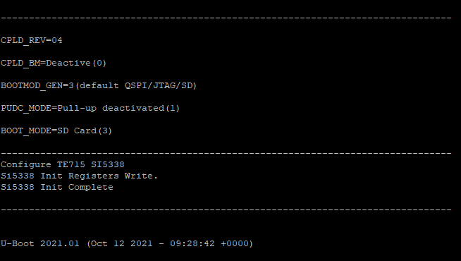
CPLD revision,boot mode and other features of the board will be shown by FSBL code in the linux console while booting.The format of these information are shown in the following:
| CPLD Revision | Software adjusted boot mode | Existed boot modes in the programmed jed File | PUDC Mode | Current boot mode | Description |
|---|---|---|---|---|---|
| Deactive (0) | 0 (QSPI/SD) | Pull-up activated (0) | JTAG (0) | ||
| Active (1) | 1 (QSPI/JTAG) | Pull-up deactivated (1) | QSPI (2) | ||
| ---- | 2 (JTAG/SD) | ---- | SD Card (3) | ||
| ---- | 3 (default QSPI/JTAG/SD) | ---- | ---- |
Boundary scan
To implement boundary scanning (especially after the production of the board is necessary to test all MIOs), MIO bank voltage must be set to a certain value.
For more information refer to the following site :https://support.xilinx.com/s/article/57930?language=en_US
From PCB revision 05 and later MIO8 state can be changed by CPLD. According the following table the MIO bank voltage can be determined for FPGA:
| Bank Voltage | Bank 1 (related pin MIO8) | Bank 0 (related pin MIO7) | Description |
|---|---|---|---|
| 2.5V / 3.3 V | 0 | 0 | MIO8 is pulled up in module hardware. MIO7 is pulled down in module hardware. |
| 1.8 V | 1 | 1 | Default value because of pull up resistor on the board |
The bank 0 voltage is determined in 2.5V / 3.3 V for FPGA by connecting MIO7 to GND. Bank 1 voltage can be determined for FPGA by changing the state of MIO8 in linux console or in FSBL code:
| Bank 1 Voltage | Command in linux console | Command in FSBL code | Description |
|---|---|---|---|
| 2.5 V / 3.3 V | i2cset -y 0 0x20 0x01 0x61 | iic_write8(0x20,0x01,0x61) | Only for boundary scaning |
| 1.8 V (Default) | ---- | ---- | MIO8 is set to high impedance. Because of pull up resistor on the board MIO8 will be set on high. |
As default MIO8 is set to high in the hardware to inform FPGA that bank 1 voltage is 1.8V. To implement boundary scan it is necessary to change MIO8 state to low. After changing the MIO8 state to low, FPGA will be reset and set in JTAG boot mode by CPLD automatically.
LED
| LED state | Description | Related command |
|---|---|---|
| Blink sequence ******** | Reset is active. (RESIN = '0') | Push reset button on the carrier board |
| Blink sequence ****oooo | Boot mode is changed by software either in linux console or by FSBL code. | i2cset -y 0 0x20 0x01 0x91 |
| Blink sequence ***ooooo | MIO8 stateis changed in linux console or in FSBL code. | i2cset -y 0 0x20 0x01 0x61 command in linux console |
| ON | Both boot mode and MIO8 state in linux console or in FSBL code are not changed. LEDs can be controlled by user too. | Default state after power on i2cset -y 0 0x20 0x03 0x00 → LED OFF |
Appx. A: Change History and Legal Notices
Revision Changes
- Changes REV03 to REV04
PGOOD is always 'Z', if anding of power good signals (pg) is high. In last version it is valid only , if BOOTMODE_GEN is not equal to 3.
LED status is changed from *****ooo state to ON state for default status.
LED can be controlled by user. For this purpose user should give the following commands:
LED ON (Default) --> i2cset -y 0 0x20 0x03 0x01
LED OFF --> i2cset -y 0 0x20 0x03 0x00
PG_MGT used as power good same as PG_3V3. (IN) This pin is unused in older versions.
- Changes REV02 to REV03
- Boot mode configuration via hardware (dip switch) and firmware added (Boot mode configuration via linux console)
- Pullup or pulldown states of PORT pins was checked.
- Adding i2c to gpio ip (i2c_slave.vhd)
- Changing oscillator frequency from 12.09 MHZ to 24.18MHZ
- PORT signals according to the schematic are renamed.
- JTAG time constraint correction.
- PGOOD pin is used as boot mode selector pin.
- VCFG1 (MIO8) pin can be changed by i2cset command. This pin must be grounded by boundary scanning.
Document Change History
To get content of older revision got to "Change History" of this page and select older document revision number.
| Date | Document Revision | CPLD Firmware Revision | Supported PCB Revision | Authors | Description |
|---|---|---|---|---|---|
| REV04 | REV05,REV04,REV03 |
| |||
2023-06-02 | v.14 | REV03 | REV05,REV04,REV03 | John Hartfiel |
|
2022-08-08 | v.13 | REV03 | REV05,REV04,REV03 | Mohsen Chamanbaz |
|
2018-07-17 | v.6 | REV02 | REV04,REV03 | John Hartfiel |
|
| 2018-07-16 | v.1 | Initial release | |||
| All |
Legal Notices
Data Privacy
Please also note our data protection declaration at https://www.trenz-electronic.de/en/Data-protection-Privacy
Document Warranty
The material contained in this document is provided “as is” and is subject to being changed at any time without notice. Trenz Electronic does not warrant the accuracy and completeness of the materials in this document. Further, to the maximum extent permitted by applicable law, Trenz Electronic disclaims all warranties, either express or implied, with regard to this document and any information contained herein, including but not limited to the implied warranties of merchantability, fitness for a particular purpose or non infringement of intellectual property. Trenz Electronic shall not be liable for errors or for incidental or consequential damages in connection with the furnishing, use, or performance of this document or of any information contained herein.
Limitation of Liability
In no event will Trenz Electronic, its suppliers, or other third parties mentioned in this document be liable for any damages whatsoever (including, without limitation, those resulting from lost profits, lost data or business interruption) arising out of the use, inability to use, or the results of use of this document, any documents linked to this document, or the materials or information contained at any or all such documents. If your use of the materials or information from this document results in the need for servicing, repair or correction of equipment or data, you assume all costs thereof.
Copyright Notice
No part of this manual may be reproduced in any form or by any means (including electronic storage and retrieval or translation into a foreign language) without prior agreement and written consent from Trenz Electronic.
Technology Licenses
The hardware / firmware / software described in this document are furnished under a license and may be used /modified / copied only in accordance with the terms of such license.
Environmental Protection
To confront directly with the responsibility toward the environment, the global community and eventually also oneself. Such a resolution should be integral part not only of everybody's life. Also enterprises shall be conscious of their social responsibility and contribute to the preservation of our common living space. That is why Trenz Electronic invests in the protection of our Environment.
REACH, RoHS and WEEE
REACH
Trenz Electronic is a manufacturer and a distributor of electronic products. It is therefore a so called downstream user in the sense of REACH. The products we supply to you are solely non-chemical products (goods). Moreover and under normal and reasonably foreseeable circumstances of application, the goods supplied to you shall not release any substance. For that, Trenz Electronic is obliged to neither register nor to provide safety data sheet. According to present knowledge and to best of our knowledge, no SVHC (Substances of Very High Concern) on the Candidate List are contained in our products. Furthermore, we will immediately and unsolicited inform our customers in compliance with REACH - Article 33 if any substance present in our goods (above a concentration of 0,1 % weight by weight) will be classified as SVHC by the European Chemicals Agency (ECHA).
RoHS
Trenz Electronic GmbH herewith declares that all its products are developed, manufactured and distributed RoHS compliant.
WEEE
Information for users within the European Union in accordance with Directive 2002/96/EC of the European Parliament and of the Council of 27 January 2003 on waste electrical and electronic equipment (WEEE).
Users of electrical and electronic equipment in private households are required not to dispose of waste electrical and electronic equipment as unsorted municipal waste and to collect such waste electrical and electronic equipment separately. By the 13 August 2005, Member States shall have ensured that systems are set up allowing final holders and distributors to return waste electrical and electronic equipment at least free of charge. Member States shall ensure the availability and accessibility of the necessary collection facilities. Separate collection is the precondition to ensure specific treatment and recycling of waste electrical and electronic equipment and is necessary to achieve the chosen level of protection of human health and the environment in the European Union. Consumers have to actively contribute to the success of such collection and the return of waste electrical and electronic equipment. Presence of hazardous substances in electrical and electronic equipment results in potential effects on the environment and human health. The symbol consisting of the crossed-out wheeled bin indicates separate collection for waste electrical and electronic equipment.
Trenz Electronic is registered under WEEE-Reg.-Nr. DE97922676.
Table of contents
Overview
Content Tools