TRM Name always "TE Series Name" +TRM, for example, "TE0720 TRM"
...
Page properties
hidden
true
id
Comments
Important General Note:
If some section is configurable and depends on Firmware, please refer to the addition page (for example CPLD). If not available, add a note, that this part is configurable
Designate all graphics and pictures with a number and a description, Use "Scroll Title" macro
Use "Scroll Title" macro for pictures and table labels. Figure number must be set manually at the moment (automatically enumeration is planned by scrollPDF)
Figure template:
Scroll Title
anchor
Figure_x
title
Figure x: Text
Scroll Ignore
Create DrawIO object here: Attention if you copy from another page, use
Scroll Only
image link to the generate DrawIO PNG file of this page. This is a workaround until a scroll pdf export bug is fixed
Table template:
Layout macro can be used for a landscape of large tables
Set column width manually(can be used for small tables to fit over the whole page) or leave empty (automatically)
Scroll Title
anchor
Table_x
title
Table x: Text
Scroll Table Layout
orientation
portrait
sortDirection
ASC
repeatTableHeaders
default
style
widths
sortByColumn
1
sortEnabled
false
cellHighlighting
true
Example
Comment
1
2
The anchors of the Scroll Title should be named consistant across TRMs. A incomplete list of examples is given below
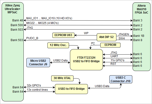
The USB 3.0 to FIFO bridge FTDI FT601Q U9 is connected to the Zynq MPSoC's PL bank 64 and is accessible through USB-C connector J10:
Scroll Title
anchor
Table_j10_10usb-c
title
Table 10: USB-C connector J10
Scroll Table Layout
orientation
portrait
sortDirection
ASC
repeatTableHeaders
default
style
widths
sortByColumn
1
sortEnabled
false
cellHighlighting
true
Interface
Signal Schematic Names
Connected to
Notes
USB3 data lane
SSRX_P
SSRX_N
SSTXX_P
SSTXX_N
USB C Connector J10
-
USB2 data lane
SS_D_P
SS_D_N
USB C Connector J10
-
Control Lines
FTDI_RESET_N
WAKEUP_N
SIWU_N
TXE_N
RXF_N
WR_N
RD_N
OE_N
BE_0
BE_1
BE_2
BE_3
FIFO_CLK
PL bank 64
-
Parallel GPIO's
DATA0
.
.
DATA31
PL bank 64
32bit FIFO register
...
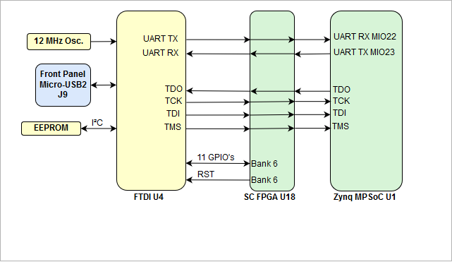
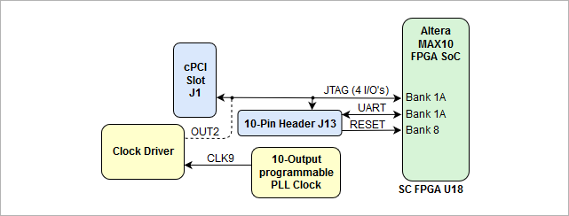
The Digilent plug-in software and cable drivers must be installed on your machine for you to be able to use JTAG interface.
Scroll Title
anchor
Figure_jtag_5uart
title
Figure 5: JTAG/UART Interface
Scroll Ignore
draw.io Diagram
border
false
viewerToolbar
true
fitWindow
false
diagramDisplayName
lbox
true
revision
8
diagramName
uart_jtag
simpleViewer
false
width
links
auto
tbstyle
hidden
diagramWidth
642
Scroll Only
The USB2 to FIFO bridge FTDI FT2232H U4 is connected to the SC FPGA U18 and is accessible through Micro-USB2 connector J9:
Scroll Title
anchor
Table_micro_11usb2
title
Table 11: Micro-USB2 connector J9
Scroll Table Layout
orientation
portrait
sortDirection
ASC
repeatTableHeaders
default
style
widths
sortByColumn
1
sortEnabled
false
cellHighlighting
true
Interface
Signal Schematic Names
Connected to
Notes
USB2 data lane
USB_P
USB_N
Micro-USB2 connector J9
-
Control Lines
FTDI_RST
SC FPGA U18, bank 6
-
Parallel GPIO's
ADBUS0
ADBUS1
ADBUS2
ADBUS3
BDBUS0
BDBUS1
BDBUS2
BDBUS3
BDBUS4
BDBUS5
BDBUS6
BDBUS7
BCBUS0
BCBUS1
BCBUS2
BCBUS3
BCBUS4
SC FPGA U18, bank 6
-
...
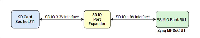
Scroll Title
anchor
Figure_6microsd
title
Figure 6: MicroSD Card interface
Scroll Ignore
draw.io Diagram
border
false
viewerToolbar
true
fitWindow
false
diagramDisplayName
lbox
true
revision
2
diagramName
TEC0850 SD IO
simpleViewer
false
width
links
auto
tbstyle
hidden
diagramWidth
641
Scroll Only
...
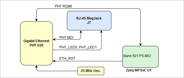
Scroll Title
anchor
Figure_7eth
title
Figure 7: Gigabit Ethernet Interface
Scroll Ignore
draw.io Diagram
border
false
viewerToolbar
true
fitWindow
false
diagramDisplayName
lbox
true
revision
2
diagramName
TEC0850 GbE
simpleViewer
false
width
links
auto
tbstyle
hidden
diagramWidth
641
Scroll Only
...
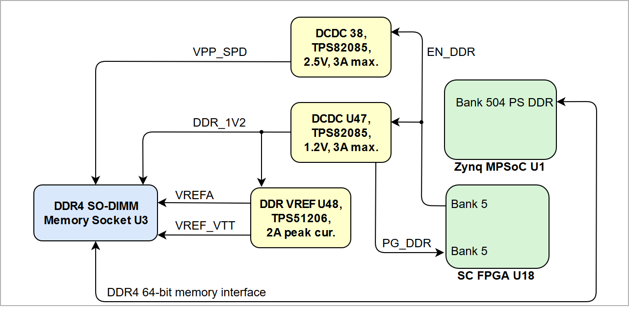
Scroll Title
anchor
Figure_8ddr4
title
Figure 8: DDR4 SDRAM SODIMM socket
Scroll Ignore
draw.io Diagram
border
false
viewerToolbar
true
fitWindow
false
diagramDisplayName
lbox
true
revision
1
diagramName
TEC0850 DDR4 interface
simpleViewer
false
width
links
auto
tbstyle
hidden
diagramWidth
641
Scroll Only
Following table gives an overview of the memory interface I/O signals of the DDR4 SDRAM SO-DIMM Socket U3:
Scroll Title
anchor
Table_12ddr4
title
Table 12: DDR4 SDRAM SO-DIMM socket U3
Scroll Table Layout
orientation
portrait
sortDirection
ASC
repeatTableHeaders
default
style
widths
sortByColumn
1
sortEnabled
false
cellHighlighting
true
DDR4 SDRAM I/O Signal
Signal Schematic Name
Connected to
Notes
Address inputs
DDR4-A0 ... DDR4-A16
PS DDR Bank 504
-
Bank address inputs
DDR4-BA0 / DDR4-BA1
-
Bank group inputs
DDR4-BG0 / DDR4-BG1
-
Differential clocks
DDR4-CLK0_P
DDR4-CLK0_N
DDR4-CLK1_P
DDR4-CLK1_N
2 x DDR4 clock
Data input/output
DQ0 ... DQ63
-
Check bit input/output
CB0 ... CB7
-
Data strobe (differential)
DDR4-DQS0_P
DDR4-DQS0_N
...
DDR4-DQS8_P
DDR4-DQS8_N
-
Data mask and data bus inversion
DDR4-DM0 ... DDR4-DM8
-
Serial address inputs
DDR4-SA0 ... DDR4-SA2
address range configuration on I²C bus
Control Signals
DDR4-CS_N0 / DDR4-CS_N1
chip select signal
DDR4-ODT0 / DDR4-ODT1
On-die termination enable
DDR4-RESET
nRESET
DDR4-PAR
Command and address parity input
DDR4-CKE0 / DDR4-CKE1
Clock Enable
DDR4-ALERT
CRC error flag
DDR4-ACT
Activation command input
DDR4-EVENT
Temperature event
I²C
DDR4-SCL
DDR4-SDA
not connected
-
...
Scroll Title
anchor
Figure_9dac
title
Figure 9: 4x 8bit DAC units
Scroll Ignore
draw.io Diagram
border
false
viewerToolbar
true
fitWindow
false
diagramDisplayName
lbox
true
revision
3
diagramName
TEC0850 DACs
simpleViewer
false
width
links
auto
tbstyle
hidden
diagramWidth
641
Scroll Only
...
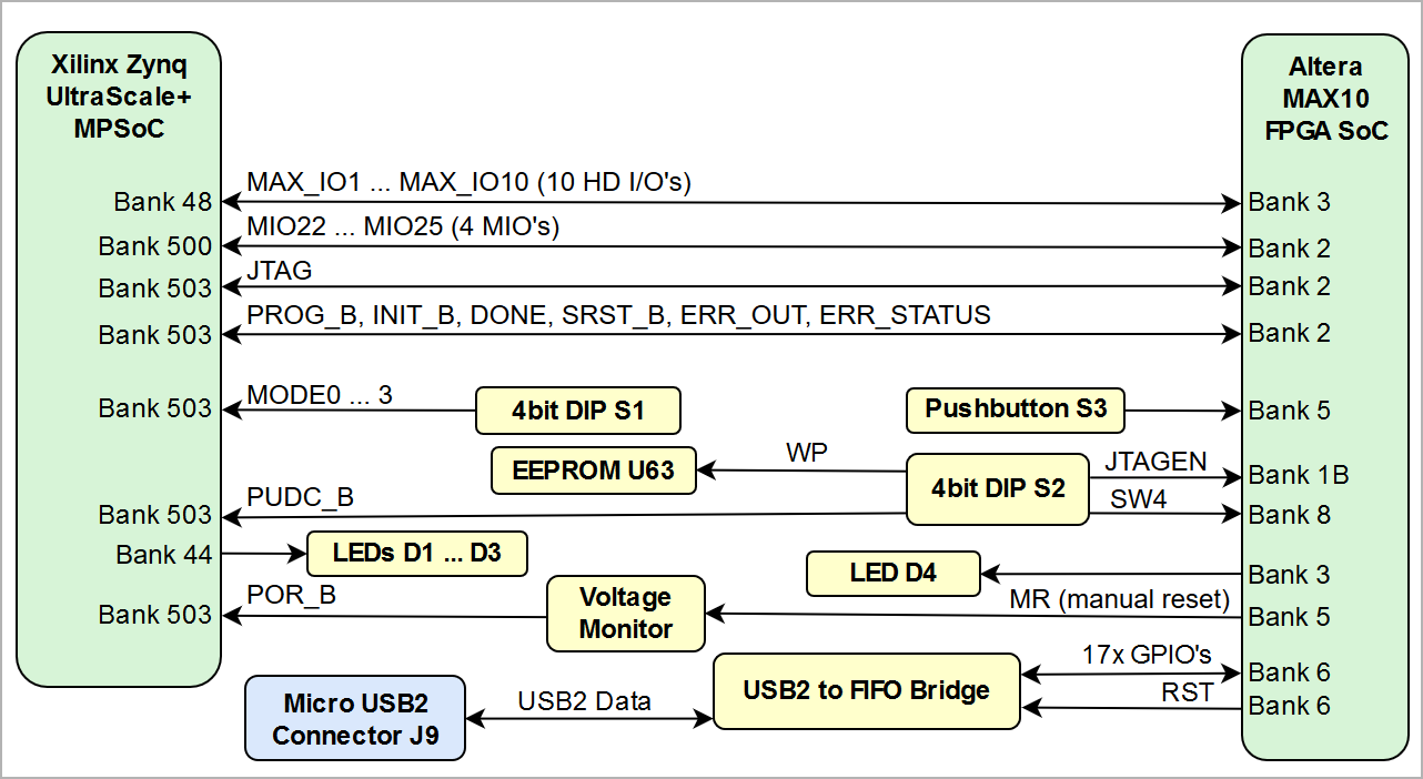
There is a 26-pin IDC header (2x13, 1.27mm grid size) J16 available on the TEC0850 board which exposes the 20 FPGA HD I/O's of PL bank 47 to the user. The PL bank 47 has 3.3V VCCO bank voltage, on the header J16 there also the voltage levels 3.3V and 5V available. The I/O's can be accessed with a corresponding IDC connector.
Scroll Title
anchor
Figure_idc_10mpsoc_pl
title
Figure 10: Zynq MPSoC PL I/O's IDC pin-header
Scroll Ignore
draw.io Diagram
border
false
viewerToolbar
true
fitWindow
false
diagramDisplayName
lbox
true
revision
3
diagramName
TEC0850 header J16
simpleViewer
false
width
links
auto
tbstyle
hidden
diagramWidth
641
Scroll Only
...
Scroll Title
anchor
Figure_1110pin_jtag_uart
title
Figure 11: 10-pin JTAG/UART header
Scroll Ignore
draw.io Diagram
border
false
viewerToolbar
true
fitWindow
false
diagramDisplayName
lbox
true
revision
3
diagramName
TEC0850 header 13
simpleViewer
false
width
links
auto
tbstyle
hidden
diagramWidth
641
Scroll Only
...
Scroll Title
anchor
Figure_123pin_picoblade
title
Figure 12: 3-pin PicoBlade header
Scroll Ignore
draw.io Diagram
border
false
viewerToolbar
true
fitWindow
false
diagramDisplayName
lbox
true
revision
1
diagramName
TEC0850 3-pin header J8
simpleViewer
false
width
links
auto
tbstyle
hidden
diagramWidth
641
Scroll Only
...
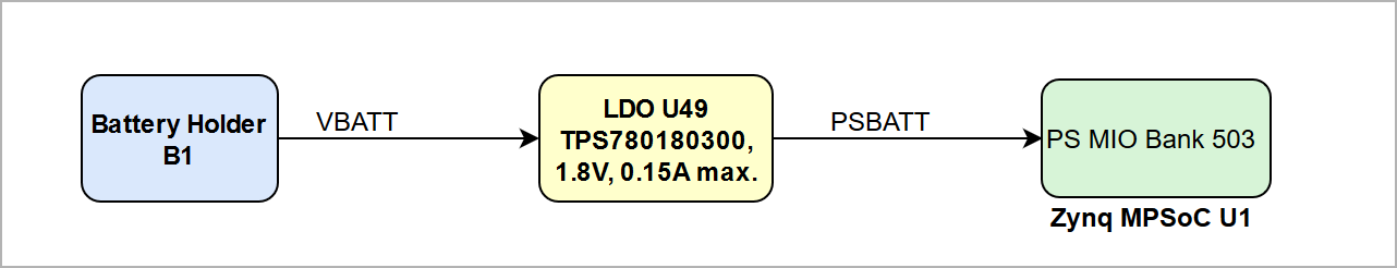
There is a CR1220 battery holder available to the supply the voltage for the Zynq MPSoC's Battery Power Domain (BBRAM and RTC). The battery voltage VBATT should be in the range of 2.2V to 5.5V, use the 3.0V CR1220 battery.
Scroll Title
anchor
Figure_Battery_13Holder
title
Figure 13: Backup-Battery Holder
Scroll Ignore
draw.io Diagram
border
false
viewerToolbar
true
fitWindow
false
diagramDisplayName
lbox
true
revision
4
diagramName
TEC0850 battery holder
simpleViewer
false
width
links
auto
tbstyle
hidden
diagramWidth
641
Scroll Only
...
Scroll Title
anchor
Figure_14fan
title
Figure 14: 4-wire PWM FAN connector
Scroll Ignore
draw.io Diagram
border
false
viewerToolbar
true
fitWindow
false
diagramDisplayName
lbox
true
revision
2
diagramName
TEC0850 4-Wire PWM Connector
simpleViewer
false
width
links
auto
tbstyle
hidden
diagramWidth
641
Scroll Only
...
The PS MIO pins are routed to the onboard peripherals as follows:
Scroll Title
anchor
Table_default_13mio
title
Table 13: Default MIO Configuration
Scroll Table Layout
orientation
portrait
sortDirection
ASC
repeatTableHeaders
default
style
widths
sortByColumn
1
sortEnabled
false
cellHighlighting
true
PS MIO
Function
Connected to
0
SPI0QSPI*
U24-B2, CLK
1
SPI0QSPI*
U24-D2, DO/IO1
2
SPI0QSPI*
U24-C4, WP/IO2
3
SPI0QSPI*
U24-D4, HOLD/IO3
4
SPI0QSPI*
U24-D3, DI/IO0
5
SPI0QSPI*
U24-C2, CS
6
-
Not not connected
7
SPI1QSPI*
U25-C2, CS
8
SPI1QSPI*
U25-D3, DI/IO0
9
SPI1QSPI*
U25-D2, DO/IO1
10
SPI1QSPI*
U17-C4, WP/IO2
11
SPI1QSPI*
U25-D4, HOLD/IO3
12
SPI1QSPI*
U25-B2, CLK
13 ... 15
-
not connected
16
USB2 PHY Reset
USB2 PHY U11, pin27
17
-
USB2 PHY Reset
USB2 PHY U13, pin27 (def. not soldered)not used
18 ... 19
-
not connected
20 ...21
PS MIO I²C
I²C peripherals
22 ... 25
user MIO
SC FPGA U18, bank 2
26 ... 38
RGMII
GbE PHY U20
39 ... 44
-
not connected
45 ... 51
SD IO
MicroSD Card socket J11
52 ... 63
USB2 ULPI
USB2 PHY U11
64 ... 75
-
USB2 ULPI
USB2 PHY U13 (def. not soldered)not used
76 ... 77
ETH MDC / MDIO
GbE PHY U20
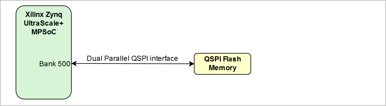
* Flash is used as QSPI dual parallel
MAX10 System Controller FPGA
...
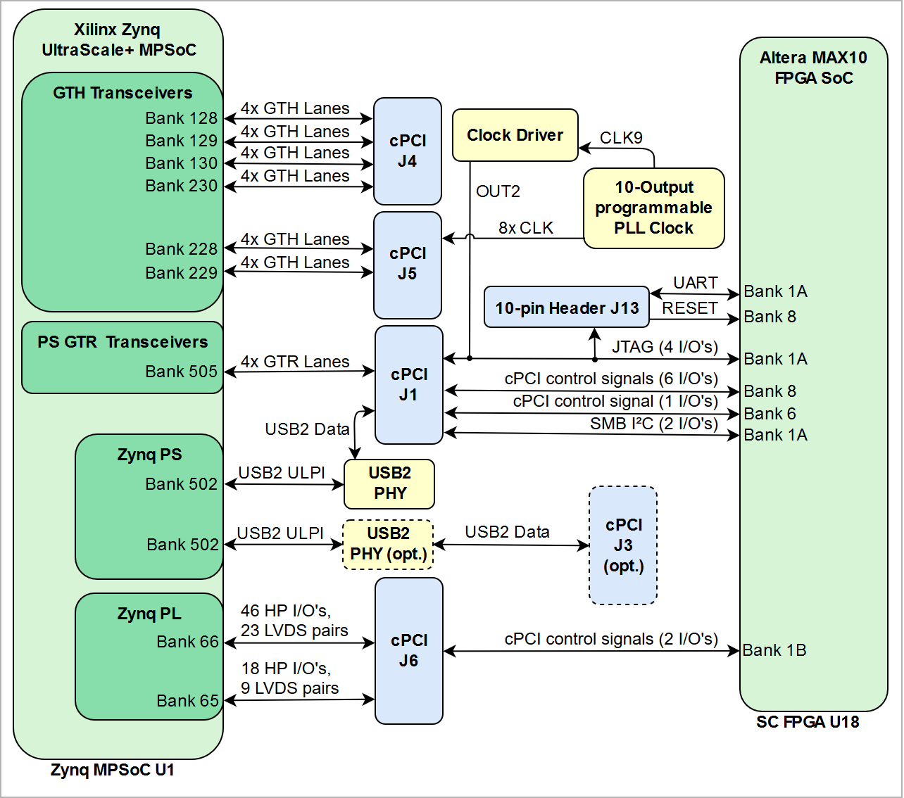
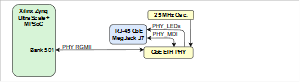
Following block diagram visualizes the connection of the SC FPGA with the Zynq Ultrascale+ MPSoC via 4 PS MIO pins (MIO22 ... 25), PS Config control signals and 10 singled ended PL HD bank 48 I/O pins (MAX_IO1 ... MAX_IO10):
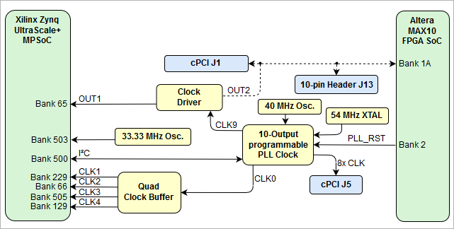
The clock generator U14 is programmable via the onboard I²C bus connected to MIO 20...21 pins. The I²C address is shown in the table below.
Scroll Title
anchor
Table_si5345_16i2c
title
Table 16: SI5345 I2C address
Scroll Table Layout
orientation
portrait
sortDirection
ASC
repeatTableHeaders
default
style
widths
sortByColumn
1
sortEnabled
false
cellHighlighting
true
I2C address
Chip
Description
0x69
U14 Si5345
Clock generator and distributor
...
The TEC0850 board is equipped several onboard oscillators to provide the Zynq Ultrascale+ MPSoC's PS and PL banks and the onboard peripherals with reference clock-signals:
Scroll Title
anchor
Table_17osc
title
Table 17: TEC0850 on-board oscillators
Scroll Table Layout
orientation
portrait
sortDirection
ASC
repeatTableHeaders
default
style
widths
sortByColumn
1
sortEnabled
false
cellHighlighting
true
Clock Source
Signal Schematic Name
Frequency
Clock Input Destination
SiTime SiT8008BI oscillator, U22
PS_CLK
33.333333 MHz
Zynq MPSoC U1 PS Config Bank 503, pin U24
SiTime SiT8008AI oscillator, U12
USB0_CLK
52.000000 MHz
USB2 transceiver PHY U11, pin 26
SiTime SiT8008AI oscillator, U16
OSCI
12.000000 MHz
FTDI FT2232H U4, pin 3
Kyocera CX3225SB30000, Y1
-
30.000 MHz
FTDI FT601Q U9, pin 21/22
CM-2012-2pad, Y2
-
32.768000 kHz
Zynq MPSoC U1 PS Config Bank 503, pin V21/V22
Kyocera CX3225SB26000, Y3
XAXB_P
XAXB_N
54.000 MHz
10-output PLL clock generator U14, pin 8/9
SiTime SiT8008BI oscillator, U21
ETH_CLKIN
25.000000 MHz
Gigabit Ethernet PHY U20, pin 34
ASVTX-12-A oscillator, U75
IN0_P
40.000 MHz
10-output PLL clock generator U14, pin 63
...
Scroll Title
anchor
Figure_17ft2232
title
Figure 17: TEC0850 on-board FTDI chips
Scroll Ignore
draw.io Diagram
border
false
viewerToolbar
true
fitWindow
false
diagramDisplayName
lbox
true
revision
4
diagramName
TEC0850 FT2232H
simpleViewer
false
width
links
auto
tbstyle
hidden
diagramWidth
641
Scroll Only
...
Channel B can be used as UART Interface routed to SC FPGA U18, 11 I/O's of Channel B is routed to are usable for example as GPIOs and other standard interfaces.
Scroll Title
anchor
Table_18ft2232
title
Table 18: FT2232H interface connections
Scroll Table Layout
orientation
portrait
sortDirection
ASC
repeatTableHeaders
default
style
widths
sortByColumn
1
sortEnabled
false
cellHighlighting
true
FT2232H U3 Pin
Signal Schematic Name
Connected to
Notes
Pin 12, ADBUS0
ADBUS0
SC FPGA U18 bank 6, pin G9
JTAG interface
Pin 13, ADBUS1
ADBUS1
SC FPGA U18 bank 6, pin F10
Pin 14, ADBUS2
ADBUS2
SC FPGA U18 bank 6, pin E10
Pin 15, ADBUS3
ADBUS3
SC FPGA U18 bank 6, pin D9
Pin 32, BDBUS0
BDBUS0
SC FPGA U18 bank 6, pin B11
UART and user configurable
GPIO's
Pin 33, BDBUS1
BDBUS1
SC FPGA U18 bank 6, pin A12
Pin 34, BDBUS2
BDBUS2
SC FPGA U18 bank 6, pin B12
Pin 35, BDBUS3
BDBUS3
SC FPGA U18 bank 6, pin C11
Pin 37, BDBUS4
BDBUS4
SC FPGA U18 bank 6, pin B13
Pin 38, BDBUS5
BDBUS5
SC FPGA U18 bank 6, pin C12
Pin 39, BDBUS6
BDBUS6
SC FPGA U18 bank 6, pin C13
Pin 40, BDBUS7
BDBUS7
SC FPGA U18 bank 6, pin D11
Pin 42, BCBUS0
BCBUS0
SC FPGA U18 bank 6, pin D12
Pin 46, BCBUS1
BCBUS1
SC FPGA U18 bank 6, pin E13
Pin 47, BCBUS2
BCBUS2
SC FPGA U18 bank 6, pin E12
Pin 48, BCBUS3
BCBUS3
SC FPGA U18 bank 6, pin F13
Pin 49, BCBUS4
BCBUS4
SC FPGA U18 bank 6, pin F12
Pin 11, nRESET
FTDI_RST
SC FPGA U18 bank 6, pin E9
control signals
...
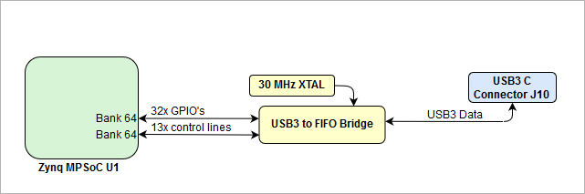
The TEC0850 board is equipped with the FTDI FT601Q USB3 to 32bit-FIFO adapter controller connected to USB-C connector J10 to provide access to the Zynq MPSoC PL HP I/O's of bank 64. Also, 13 control signals of the FTDI FT601Q are connected to the HP bank 64.
Scroll Title
anchor
Table_19ft601q
title
Table 19: FT601Q interface connections
Scroll Table Layout
orientation
portrait
sortDirection
ASC
repeatTableHeaders
default
style
widths
sortByColumn
1
sortEnabled
false
cellHighlighting
true
FT601Q U9 Pin
Signal Schematic Name
Connected to
Notes
Pin 40, DATA0
DATA0
PL HP bank 64, pin AK1
user GPIO's
Pin 41, DATA1
DATA1
PL HP bank 64, pin AJ10
Pin 42, DATA2
DATA2
PL HP bank 64, pin AJ9
Pin 43, DATA3
DATA3
PL HP bank 64, pin AK7
Pin 44, DATA4
DATA4
PL HP bank 64, pin AK5
Pin 45, DATA5
DATA5
PL HP bank 64, pin AM1
Pin 46, DATA6
DATA6
PL HP bank 64, pin AL2
Pin 47, DATA7
DATA7
PL HP bank 64, pin AK4
Pin 50, DATA8
DATA8
PL HP bank 64, pin AN1
Pin 51, DATA9
DATA9
PL HP bank 64, pin AL3
Pin 52, DATA10
DATA10
PL HP bank 64, pin AK8
Pin 53, DATA11
DATA11
PL HP bank 64, pin AN2
Pin 54, DATA12
DATA12
PL HP bank 64, pin AP2
Pin 55, DATA13
DATA13
PL HP bank 64, pin AL7
Pin 56, DATA14
DATA14
PL HP bank 64, pin AL5
Pin 57, DATA15
DATA15
PL HP bank 64, pin AM4
Pin 60, DATA16
DATA16
PL HP bank 64, pin AN4
Pin 61, DATA17
DATA17
PL HP bank 64, pin AM5
Pin 62, DATA18
DATA18
PL HP bank 64, pin AM6
Pin 63, DATA19
DATA19
PL HP bank 64, pin AN3
Pin 64, DATA20
DATA20
PL HP bank 64, pin AP3
Pin 65, DATA21
DATA21
PL HP bank 64, pin AP4
Pin 66, DATA22
DATA22
PL HP bank 64, pin AP5
Pin 67, DATA23
DATA23
PL HP bank 64, pin AN6
Pin 69, DATA24
DATA24
PL HP bank 64, pin AN7
Pin 70, DATA25
DATA25
PL HP bank 64, pin AP6
Pin 71, DATA26
DATA26
PL HP bank 64, pin AP7
Pin 72, DATA27
DATA27
PL HP bank 64, pin AP11
Pin 73, DATA28
DATA28
PL HP bank 64, pin AP10
Pin 74, DATA29
DATA29
PL HP bank 64, pin AP9
Pin 75, DATA30
DATA30
PL HP bank 64, pin AN9
Pin 76, DATA31
DATA31
PL HP bank 64, pin AP8
Pin 58, CLK
FIFO_CLK
PL HP bank 64, pin AL6
control signals
Pin 4, BE0
BE_0
PL HP bank 64, pin AM10
Pin 5, BE1
BE_1
PL HP bank 64, pin AK10
Pin 6, BE2
BE_2
PL HP bank 64, pin AM11
Pin 7, BE3
BE_3
PL HP bank 64, pin AL11
Pin 13, nOE
OE_N
PL HP bank 64, pin AL8
Pin 12, nRD
RD_N
PL HP bank 64, pin AK9
Pin 11, nWR
WR_N
PL HP bank 64, pin AM9
Pin 8, nTXE
TXE_N
PL HP bank 64, pin AK12
Pin 9, nRXN
RXF_N
PL HP bank 64, pin AJ12
Pin 10, nSIWU
SIWU_N
PL HP bank 64, pin AL10
Pin 15, nRESET
FTDI_RESET_N
PL HP bank 64, pin AM8
Pin 16, nWAKEUP
WAKEUP_N
PL HP bank 64, pin AN8
...
Scroll Title
anchor
Figure_18qspi
title
Figure 18: Quad-SPI Flash Memory
Scroll Ignore
draw.io Diagram
border
false
viewerToolbar
true
fitWindow
false
diagramDisplayName
lbox
true
revision
1
diagramName
TEC0850 QSPI Flash
simpleViewer
false
width
links
auto
tbstyle
hidden
diagramWidth
641
Scroll Only
...
Scroll Title
anchor
Figure_19eeprom
title
Figure 19: On-board configuration EEPROMs
Scroll Ignore
draw.io Diagram
border
false
viewerToolbar
true
fitWindow
false
diagramDisplayName
lbox
true
revision
2
diagramName
TEC0850 USB3 to FIFO
simpleViewer
false
width
links
auto
tbstyle
hidden
diagramWidth
641
Scroll Only
...
The EEPROMs U63 and U64 are programmable via the onboard I²C bus connected to MIO 20...21 pins. The I²C address is shown in the table below.
Scroll Title
anchor
Table_eeprom_21i2c
title
Table 21: EEPROMs I²C Addresses
Scroll Table Layout
orientation
portrait
sortDirection
ASC
repeatTableHeaders
default
style
widths
sortByColumn
1
sortEnabled
false
cellHighlighting
true
I2C address
Chip
Description
0x50
U63 24AA128T-I/ST
128K Serial EEPROM
0x53
U64 24AA025E48T-I/OT
2K Serial EEPROM with EUI-48™ or EUI-64™ Node Identity
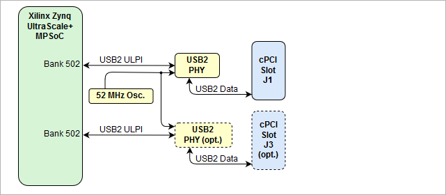
USB2 PHY
USB2 PHY U15 U11 is provided by USB3320 from Microchip. The ULPI interface is connected to the Zynq Ultrascale+ PS USB0. I/O voltage is fixed at 1.8V and PHY reference clock input is supplied from the on-board 52.000000 MHz oscillator U12.
Scroll Title
anchor
Figure_20usb2_phy
title
Figure 20: TEC0850 cPCI USB2 interface
Scroll Ignore
draw.io Diagram
border
false
viewerToolbar
true
fitWindow
false
diagramDisplayName
lbox
true
revision
1
diagramName
TEC0850 USB2 PHY
simpleViewer
false
width
links
auto
tbstyle
hidden
diagramWidth
641
Scroll Only
Scroll Title
anchor
Table_22usb2_phy_io
title
Table 22: USB2 ULPI interface description
Scroll Table Layout
orientation
portrait
sortDirection
ASC
repeatTableHeaders
default
style
widths
sortByColumn
1
sortEnabled
false
cellHighlighting
true
PHY Pin
Connected to
Notes
ULPI
PS bank MIO52 ... MIO63
Zynq Ultrascale+ USB0 MIO pins are connected to the PHY
REFCLK
-
52MHz from onboard oscillator U12
REFSEL[0..2]
-
All pins set to GND selects the external reference clock frequency (52.000000 MHz)
RESETB
Zynq MPSoC MIO16, pin AM16
Low active USB2 PHY Reset
DP, DM
cPCI connector J1
USB2 data lane
CPEN
-
External USB power switch active-high enable signal
VBUS
5V
Connected to USB VBUS via a series of resistors, see schematic
ID
3.3V
B-device
...
Scroll Title
anchor
Figure_21eth_phy
title
Figure 21: TEC0850 GbE interface with RJ-45 MegJack
Scroll Ignore
draw.io Diagram
border
false
viewerToolbar
true
fitWindow
false
diagramDisplayName
lbox
true
revision
1
diagramName
TEC0850 GbE PHY
simpleViewer
false
width
links
auto
tbstyle
hidden
diagramWidth
641
Scroll Only
...
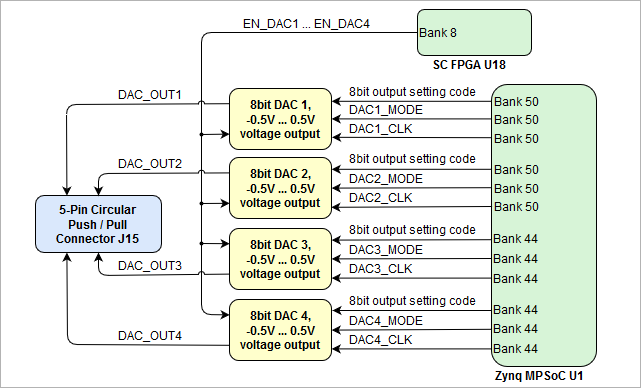
The TEC0850 Board has 4 8-bit parallel Texas Instruments THS5641AIPW digital to analog converter (DAC) with up to 100 MSPS update rate connected to TI THS4631D operational amplifiers. See Schematic circuitry and TI THS5641 data sheet for proper operation of the on-board DAC units.
Scroll Title
anchor
Table_dac_23io
title
Table 23: DAC units interface description
Scroll Table Layout
orientation
portrait
sortDirection
ASC
repeatTableHeaders
default
style
widths
sortByColumn
1
sortEnabled
false
cellHighlighting
true
DAC unit
Signal Schematic Name
Connected to
Functionality
DAC1
U28
DAC1_D0
PL HD bank 50, pin D11
Digital input bits D[7:0]
D7 is the most significant data bit (MSB), D0 is the least significant data bit (LSB).
DAC1_D1
PL HD bank 50, pin D10
DAC1_D2
PL HD bank 50, pin G11
DAC1_D3
PL HD bank 50, pin J11
DAC1_D4
PL HD bank 50, pin G10
DAC1_D5
PL HD bank 50, pin H10
DAC1_D6
PL HD bank 50, pin J10
DAC1_D7
PL HD bank 50, pin E10
DAC1_CLK
PL HD bank 50, pin F12
External clock input, input data latched on rising edge of the clock.
DAC1_MODE
PL HD bank 50, pin F10
Input code format (binary, twos complement)
EN_DAC1
SC FPGA U18 bank 8, pinE6
generate 3.3V voltages LDO U35, U34
DAC2
U31
DAC2_D0
PL HD bank 50, pin G15
Digital input bits D[7:0]
D7 is the most significant data bit (MSB), D0 is the least significant data bit (LSB).
DAC2_D1
PL HD bank 50, pin H14
DAC2_D2
PL HD bank 50, pin J14
DAC2_D3
PL HD bank 50, pin G14
DAC2_D4
PL HD bank 50, pin G13
DAC2_D5
PL HD bank 50, pin H13
DAC2_D6
PL HD bank 50, pin H12
DAC2_D7
PL HD bank 50, pin J12
DAC2_CLK
PL HD bank 50, pin F12
External clock input, input data latched on rising edge of the clock.
DAC2_MODE
PL HD bank 50, pin F11
Input code format (binary, twos complement)
EN_DAC2
SC FPGA U18 bank 8, pin E8
generate 3.3V voltages LDO U32, U60
DAC3
U29
DAC3_D0
PL HD bank 44, pin AG14
Digital input bits D[7:0]
D7 is the most significant data bit (MSB), D0 is the least significant data bit (LSB).
DAC3_D1
PL HD bank 44, pin AE13
DAC3_D2
PL HD bank 44, pin AG13
DAC3_D3
PL HD bank 44, pin AJ15
DAC3_D4
PL HD bank 44, pin AJ14
DAC3_D5
PL HD bank 44, pin AH14
DAC3_D6
PL HD bank 44, pin AL13
DAC3_D7
PL HD bank 44, pin AM13
DAC3_CLK
PL HD bank 44, pin AK15
External clock input, input data latched on rising edge of the clock.
DAC3_MODE
PL HD bank 44, pin AK14
Input code format (binary, twos complement)
EN_DAC3
SC FPGA U18 bank 8, pin B6
generate 3.3V voltages LDO U66, U68
DAC4
U33
DAC4_D0
PL HD bank 44, pin AP14
Digital input bits D[7:0]
D7 is the most significant data bit (MSB), D0 is the least significant data bit (LSB).
DAC4_D1
PL HD bank 44, pin AN14
DAC4_D2
PL HD bank 44, pin AM14
DAC4_D3
PL HD bank 44, pin AN13
DAC4_D4
PL HD bank 44, pin AP12
DAC4_D5
PL HD bank 44, pin AN12
DAC4_D6
PL HD bank 44, pin AF13
DAC4_D7
PL HD bank 44, pin AH13
DAC4_CLK
PL HD bank 44, pin AK13
External clock input, input data latched on rising edge of the clock.
DAC4_MODE
PL HD bank 44, pin AK13
Input code format (binary, twos complement)
EN_DAC4
SC FPGA U18 bank 8, pin A6
generate 3.3V voltages LDO U70, U72
...
The table below describes the functionalities of the switches of DIP-switches S1 and S2 at their every position:
The TEC0850 board is equipped with several LEDs to signal current states and activities.
Scroll Title
anchor
Table_26leds
title
Table 26: On-board LEDs description
Scroll Table Layout
orientation
portrait
sortDirection
ASC
repeatTableHeaders
default
style
widths
sortByColumn
1
sortEnabled
false
cellHighlighting
true
LED
Color
Connected to
Description and Notes
Front panel LED D1
Red
Zynq MPSoC PL bank 11, pin AF15
PL User defined LED
Front panel LED D2
Green
Zynq MPSoC PL bank 11, pin AG15
PL User defined LED
Front panel LED D3
Green
Zynq MPSoC PL bank 11, pin AE15
PL User defined LED
Front panel LED D4
Green
SC FPGA U18 bank 3, pin M4
Power Good
...
Xilinx provides a power estimator excel sheets to calculate power consumption. It's also possible to evaluate the power consumption of the developed design with Vivado. See also Trenz Electronic Wiki FAQ.
Scroll Title
anchor
Table_PWR_27PC
title
Table 27: Typical power consumption
Scroll Table Layout
orientation
portrait
sortDirection
ASC
repeatTableHeaders
default
style
widths
sortByColumn
1
sortEnabled
false
cellHighlighting
true
Power Input
Typical Current
VIN_12V
TBD*
...
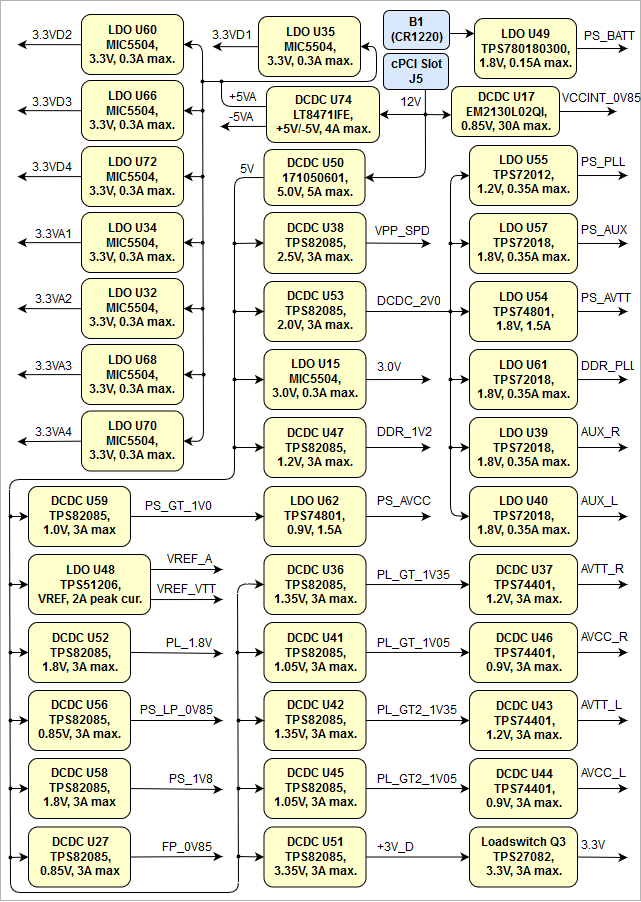
There are following dependencies how the initial 24V voltage from the main power pins on cPCI slot J1 is distributed to the onboard DC-DC converters, which power up further DC-DC converters and the particular on-board voltages:
Scroll Title
anchor
Figure_PWR_22PD
title
Figure 22: Power Distribution
Scroll Ignore
draw.io Diagram
border
false
viewerToolbar
true
fitWindow
false
diagramDisplayName
lbox
true
revision
16
diagramName
Power supply
simpleViewer
false
width
links
auto
tbstyle
hidden
diagramWidth
641
Scroll Only
...
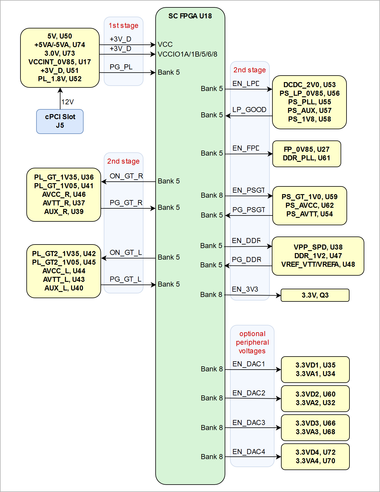
Following diagram describes the sequence of enabling the three power instances utilizing the DC-DC converter control signals (Enable, Power-Good), which will power-up in descending order as listed in the blocks of the diagram.
Scroll Title
anchor
Figure_PWR_23PS
title
Figure 23: Power-On Sequence Diagram
Scroll Ignore
draw.io Diagram
border
false
viewerToolbar
true
fitWindow
false
diagramDisplayName
lbox
true
revision
2
diagramName
TEC0850 Power-On Sequence Diagram
simpleViewer
false
width
links
auto
tbstyle
hidden
diagramWidth
641
Scroll Only
...
Scroll Title
anchor
Figure_24PWR_PM
title
Figure 24: TEC0850 voltage monitor circuit
Scroll Ignore
draw.io Diagram
border
false
viewerToolbar
true
fitWindow
false
diagramDisplayName
lbox
true
revision
1
diagramName
TEC0850 Voltage Monitor Circuit
simpleViewer
false
width
links
auto
tbstyle
hidden
diagramWidth
642
Scroll Only
Power Rails
Scroll Title
anchor
Table_28PWR_PR
title
Table 28: TEC0850 power rails description
Scroll Table Layout
orientation
portrait
sortDirection
ASC
repeatTableHeaders
default
style
widths
sortByColumn
1
sortEnabled
false
cellHighlighting
true
Connector / Pin
Voltage
Direction
Notes
J1, pin A1, D1, E1, G1, H1, J1, K1
VIN_12V
Input
Main power supply pins
J17, pin 2
12V
Output
4-wire PWM fan connector supply voltage
J13, pin 4
+3V_D
Output
JTAG/UART reference VCCIO voltage
B1, pin +
VBATT
Input
3.0V CR1220 battery
J16, pin 2
5V
Output
I/O header VCCIO
J16, pin 1
3.3V
Output
I/O header VCCIO
J9, pin 4
VBUS
Input
USB2 VBUS (5.0V nominal)
J10, pin A4, B9
VBUS30
Input
USB3 VBUS (5.0V nominal)
J11, pin 4
3.3V
Output
MicroSD Card VDD
J15, pin 2
DAC1_OUT
Output
DAC output
J15, pin 3
DAC2_OUT
Output
DAC output
J15, pin 4
DAC3_OUT
Output
DAC output
J15, pin 5
DAC4_OUT
Output
DAC output
Bank Voltages
Scroll Title
anchor
Table_PWR_29BV
title
Table 29: TEC0850 Zynq MPSoC and SC FPGA bank voltages
Scroll Table Layout
orientation
portrait
sortDirection
ASC
repeatTableHeaders
default
style
widths
sortByColumn
1
sortEnabled
false
cellHighlighting
true
Zynq MPSoC Bank
Type
Schematic Name
Voltage
Voltage Range
44
HD
3.3V
3.3V
fixed to 3.3V
47
HD
3.3V
3.3V
fixed to 3.3V
48
HD
3.3V
3.3V
fixed to 3.3V
49
HD
3.3V
3.3V
fixed to 3.3V
50
HD
3.3V
3.3V
fixed to 3.3V
64
HP
PL_1V8
1.8V
fixed to 1.8V
65
HP
PL_1V8
1.8V
fixed to 1.8V
66
HP
PL_1V8
1.8V
fixed to 1.8V
67
HP
PL_1V8
1.8V
fixed to 1.8V
500
MIO
PS_1V8
1.8V
fixed to 1.8V
501
MIO
PS_1V8
1.8V
fixed to 1.8V
502
MIO
PS_1V8
1.8V
fixed to 1.8V
503
CONFIG
PS_1V8
1.8V
fixed to 1.8V
504
PSDDR
DDR_1V2 DDR_PLL
1.2V 1.8V
fixed bank voltages
128
129
130
GTH
AVCC_L
AUX_L
AVTT_L
0.9V
1.8V
1.2V
fixed bank voltages
228
229
230
GTH
AVCC_R
AUX_R
AVTT_R
0.9V
1.8V
1.2V
fixed bank voltages
MAX10 FPGA Bank
Type
Schematic Name
Voltage
Voltage Range
1A
-
+3V_D
3.3V
fixed to 3.3V
1B
-
+3V_D
3.3V
fixed to 3.3V
2
-
PS_1V8
1.8V
fixed to 1.8V
3
-
3.3V
3.3V
fixed to 3.3V
5
-
+3V_D
3.3V
fixed to 3.3V
6
-
+3V_D
3.3V
fixed to 3.3V
8
-
+3V_D
3.3V
fixed to 3.3V
...
Absolute Maximum Ratings
Scroll Title
anchor
Table_30AMR
title
Table 30: Module absolute maximum ratings
Scroll Table Layout
orientation
portrait
sortDirection
ASC
repeatTableHeaders
default
style
widths
sortByColumn
1
sortEnabled
false
cellHighlighting
true
Parameter
Min
Max
Unit
Reference Document
Notes
VIN_12V
-0.3
16
V
Intel Enpirion EM2130 data sheet / Fuse F1
Fuse F1 @16V/2.5A
VBATT
-0.3
6
V
TPS780180300 data sheet
1.8V typical output
VCCO for HD I/O banks
-0.5
3.4
V
Xilinx document DS925
-
VCCO for HP I/O banks
-0.5
2
V
Xilinx document DS925
-
I/O input voltage for HD I/O banks
-0.55
VCCO + 0.55
V
Xilinx document DS925
-
I/O input voltage for HP I/O banks
-0.55
VCCO + 0.55
V
Xilinx document DS925
-
PS I/O input voltage (MIO pins)
-0.5
VCCO_PSIO + 0.55
V
Xilinx document DS925
VCCO_PSIO 1.8V nominally
PS GTR reference clocks absolute input voltage
-0.5
1.1
V
Xilinx document DS925
-
PS GTR absolute input voltage
-0.5
1.1
V
Xilinx document DS925
-
MGT clock absolute input voltage
-0.5
1.3
V
Xilinx document DS925
-
MGT Receiver (RXP/RXN) and transmitter (TXP/TXN) absolute input voltage
-0.5
1.2
V
Xilinx document DS925
-
SC FPGA U18 I/O input voltage
-0.5
VCC + 0.5
V
Intel MAX 10 data sheet
VCC 3.3V nominally
A voltage on input I/O pins of DC-DC U17 EM2130 on header J12
-0.3
3.6
V
Intel Enpirion EM2130 datasheet
-
Storage temperature (ambient)
-40
85
°C
ASVTX-12 datasheet
-
Recommended Operating Conditions
Scroll Title
anchor
Table_31ROC
title
Table 31: Module absolute maximum ratings
Scroll Table Layout
orientation
portrait
sortDirection
ASC
repeatTableHeaders
default
style
widths
sortByColumn
1
sortEnabled
false
cellHighlighting
true
Parameter
Min
Max
Unit
Reference Document
Notes
VIN_12V
12
14
V
Intel Enpirion EM2130 datasheet
12V nominally input voltage
VBATT
2.2
5.5
V
TPS780180300 data sheet
supplied by 3.0V CR1220 battery
VCCO for HD I/O banks
1.14
3.4
V
Xilinx document DS925
-
VCCO for HP I/O banks
0.95
1.9
V
Xilinx document DS925
-
I/O input voltage for HD I/O banks
-0.2
VCCO + 0.2
V
Xilinx document DS925
-
I/O input voltage for HP I/O banks
-0.2
VCCO + 0.2
V
Xilinx document DS925
-
PS I/O input voltage (MIO pins)
-0.2
VCCO_PSIO + 0.2
V
Xilinx document DS925
VCCO_PSIO 1.8V nominally
SC FPGA U18 I/O input voltage
0
VCC
V
Intel MAX 10 data sheet
VCC 3.3V nominally
Board Operating Temperature Range 1), 2)
0
85
°C
Xilinx document DS925
extended grade Zynq MPSoC temperature range
...
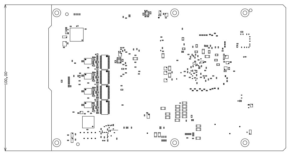
Scroll Title
anchor
Figure_25PD
title
Figure 25: Physical dimensions drawing
...
Page properties
hidden
true
id
Comments
Set correct link to the shop page overview table of the product on English and German, if not available, set
Note this list must be only updated if the document is online on public doc!
It's semi-automatically, so do the following
Add new row below first
Copy "Page Information Macro(date)" Macro-Preview, Metadata Version number, Author Name and description to the empty row. Important Revision number must be the same as the Wiki document revision number Update Metadata = "Page Information Macro (current-version)" Preview+1 and add Author and change description. --> this point it will be deleted on newer pdf export template
Metadata is only used for compatibility of older exports