Page History
...
| HTML |
|---|
<!-- Template Revision 1.6 (HTML comments will be not displayed in the document, no need to remove them. For Template/Skeleton changes, increase Template Revision number. So we can check faster, if the TRM style is up to date). --> |
| Scroll Ignore |
|---|
| Scroll pdf ignore | |
|---|---|
Table of Contents
|
Overview
| Scroll Only (inline) |
|---|
Refer to https://wiki.trenz-electronic.de/display/PD/TE0741 for online version of this manual and the rest of available documentation.
|
Trenz Electronic TE0741 is an industrial-grade FPGA module integrating a Xilinx Kintex-7 FPGA, 32 MByte SPI Flash memory for configuration and operation, and powerful switching-mode power supplies for all on-board voltages. A large number of configurable I/Os is provided via rugged high-speed stacking strips.
The TE0741 module is available in four different logic densities (70T, 160T, 325T and 410T). The 70T and 160T devices can be programmed with the free Xilinx Vivado WebPACK software. Further information about the Kintex-7 FPGA can be found in the Xilinx document 7 Series FPGA's Overview (DS180).
Key Features
| Scroll Only (inline) |
|---|
Refer to http://trenz.org/te0741-info for online version of this manual and the rest of available documentation. |
Key Features
- Industrial-grade Xilinx Kintex-7 FPGA Industrial-grade Xilinx Kintex-7 FPGA module (70T*, 160T*, 325T, 410T)
* Devices supported by the free Xilinx Vivado WebPACK software. - 256-Mbit (32-MByte) Quad SPI Flash memory (for configuration and operation) accessible through:
- FPGA
- JTAG port (SPI indirect (Bus width x4))
- 8 GTX transceivers
- FPGA configuration through:
- JTAG (B2B connector)
- SPI Flash memory
- 25 MHz low jitter oscillator with shutdown control
- Programmable quad PLL clock generator
- On-board high-efficiency DC-DC converters
- GTX voltage regulators with control enable
- Core voltage regulator: 20A (2 x Enpirion DC-DC regulators with load-sharing)
- Supply voltages: either 3.3V or 3.3V and 5V
- Plug-on module with two 100-pin and one 60-pin high-speed hermaphroditic stacking strips
- Up to 144 (94 for 70T) FPGA I/O pins are available on B2B strips (up to 65 LVDS pairs possible)
- 2 user LED's, 1x DONE FPGA pin LED, 1 System Controller status LED
- System management and power sequencing
- AES bit-stream encryption
- eFUSE bit-stream encryption
- Evenly spread supply pins for good signal integrity
...
| Pin Name | Mode | Function | Default Configuration | B2B Connector |
|---|---|---|---|---|
| PGOOD | OutputINOUT | Power Good | Active high low when all on-module power supplies are working properly.failed, otherwise high impedance | JM1-30 |
| RESIN | Input | Reset | Active low reset signal, drive low to keep the system in reset (FPGA pin PROG_B will be driven by CPLD). | JM2-18 |
| JTAGMODE | Input | JTAG Select | Low for normal operation, high (3.3V) to program the System Controller CPLD. | JM1-89 |
Table 4: Pin-description of System Controller CPLD. Important, functionality depends on CPLD Firmware, see TE0741 CPLD. General 4x5 module controller IO description on 4 x 5 SoM Integration Guide#4x5SoMIntegrationGuide-4x5ModuleControllerIOs
On-On-board LEDs
There are four LED's available on TE0741 SoM. Two status LED's (D3 and D4) and two user configurable LED's (D1 and D2).
| LED | Color | Connected to | Description and Notes |
|---|---|---|---|
| D1 | Green | LED2 | User configurable LED. |
| D2 | Red | LED1 | User configurable LED. |
| D3 | Green | DONE | Reflects inverted DONE signal, ON when FPGA is not configured, OFF as soon as PL is configured. This LED will not operate if the the 3.3V power rail is not available. After FPGA configuration the user can use USRACCESSE2 to control Done LED. |
| D4 | Green | C_LED | Connected to the system controller indicating status of the module, functionalitly, see: TE0741 CPLD#LED Steadily lit: RESIN pin is kept low. Blinking fast (0.1s on/off): Power sequencing fault (PG_ALL = 0). Blinking at medium speed (0.5s on/off): Power sequencing has completed but the FPGA is not configured (PG_ALL = 1, DONE = 0). Blinking slow (1s on/off): FPGA is configured and board is ready (PG_ALL = 1, DONE = 1). It is also possible to program the System Controller CPLD to connect this LED to FPGA pin named XIO. |
Table 5: Description of the on board LED's.
Table 5: Description of the on board LED's.
Note: if FPGA logic toggles DONE pin (to control D3) Note: if FPGA logic toggles DONE pin (to control D3) then D4 will toggle at random, as changing value on DONE will change the blink frequency of D4.
...
Figure 3: Clocking block diagram.
| I/O Si5338A (U2) | Default Frequency | Notes |
|---|---|---|
IN1/IN2 | - | Not used (external clock signal supply). |
IN3 | 25MHz | Fixed input clock signal from. reference clock generator SiT8208AI (U3). |
IN4 | - | LSB of the default I2C-Adress 0x70. |
IN5/IN6 | - | Not used (external clock signal supply). |
CLK0 A/B | 100 MHz | Bank 14 clock input, Pins: B14_L12_P, B14_L12_N |
CLK1 A/B | 125MHz | MGT reference clock 1 to FPGA Bank 116 MGT |
CLK2 A/B | - | MGT reference clock 3 to FPGA Bank 115 MGT |
| CLK3 | - | not used |
...
To enable the voltage supply for the GTX transceivers, namely the Enpirion EP53F8QI voltage regulators U6 and U16, which serve the voltages MGTAVCC (1.0 V) and MGTAVTT (1.2 V), the signal EN_MGT (bank 14, pin H22) have to be set high. The voltage regulators will indicate "Power OK" with signals PG_MGT_1V and PG_MGT_1V2, when reaching stable state.
![]()
Figure 4: GTX transceiver block diagram.
...
Green LED D4 (C_LED) connected to the System Controller CPLD is to indicate the status of the module. CPLD Firmware, see TE0741 CPLD.
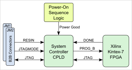
Figure 5: System Controller CPLD block diagram.
...
Board to Board Connectors
| Include Page | ||||||
|---|---|---|---|---|---|---|
|
Variants Currently In Production
...
| Date | Revision | Notes | PCN | Documentation | ||
|---|---|---|---|---|---|---|
| 2016-10-25 | 03 | 1) Fixed DC-DC connection for parallel operation 2) Samtec Razor Beam connectors updated 3) Serial number (traceability) pad added 4) Changed ferrite beads L1..L4 size 0402 to BKP0603HS121-T 5) Thermal vias added to mounting holes | PCN-20170106 | TE0741-03 | ||
| 2013-11-06 | 02 |
| TE0741-02 | |||
| 01 | First production release |
Hardware revision number is written on the PCB board together with the module model number separated by the dash.
...
Document Change History
| Date | Revision | Contributors | DescriptionRevision | Contributors | Description | ||||||||||||||||||||||||||
|---|---|---|---|---|---|---|---|---|---|---|---|---|---|---|---|---|---|---|---|---|---|---|---|---|---|---|---|---|---|---|---|
|
|
|
| ||||||||||||||||||||||||||||
| 2018-08-29 | v.64 | John Hartfiel |
| ||||||||||||||||||||||||||||
2017-11-10 | v.63 | John Hartfiel |
| ||||||||||||||||||||||||||||
| 2017-08-28 | v.60 | Jan Kumann |
| ||||||||||||||||||||||||||||
| 2017-07-20 | v.57 | John Hartfiel |
| ||||||||||||||||||||||||||||
| 2017-06-07 | v.55 | Jan Kumann |
| ||||||||||||||||||||||||||||
| 2017-06-02 | v.50 | Jan Kumann |
| ||||||||||||||||||||||||||||
| 2017-01-22 | v.42 | Jan Kumann |
| ||||||||||||||||||||||||||||
| 2017-01-13 | v.38 | Jan Kumann |
| ||||||||||||||||||||||||||||
| 2017-01-12 | v.21 | John Hartfiel |
| ||||||||||||||||||||||||||||
| 2016-12-14 | v.19 | Ali Naseri |
| ||||||||||||||||||||||||||||
| 2013-12-02 | v.1 | Antti Lukats, Jon Bean |
|
Disclaimer
| Include Page | ||||
|---|---|---|---|---|
|
Overview
Content Tools