...
| Scroll Title |
|---|
| anchor | Figure_OV_MC |
|---|
| title | TE0835 main components |
|---|
|
| Scroll Ignore |
|---|
| draw.io Diagram |
|---|
| border | false |
|---|
| viewerToolbar | true |
|---|
| |
|---|
| fitWindow | false |
|---|
| diagramDisplayName | |
|---|
| lbox | true |
|---|
| revision | 1718 |
|---|
| diagramName | TE0835_OV_MC |
|---|
| simpleViewer | false |
|---|
| width | 639 |
|---|
| links | auto |
|---|
| tbstyle | hidden |
|---|
| diagramWidth | 641 |
|---|
|
|
| Scroll Only |
|---|
|
|
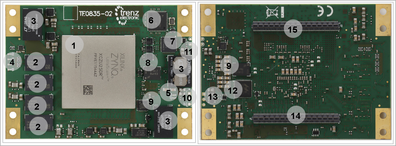
- Xilinx UltraScale+ RFSoC XCZU25DRRFSoC, U1
- 8Gb DDR4 SDRAM, U2,U3,U5,U9
- Voltage Regulators, U4,U6,U7
- User Red LEDs, D2...5
- Error/Status Red LEDs, D6...7
- Programmable Glock Generator, U15
- Lattice MachXO2 CPLD, U31
- Dual SPI Flash, U24-U25
- USB2.0 Transceiver, U11
- Pin Header 3x1, J3 (not Soldered)
- Gigabit Ethernet Transceiver, U20
- EEPROM, U23
- B2B Connectors, J1
- B2B Connectors, - J2
Initial Delivery State
| Page properties |
|---|
|
Notes : Only components like EEPROM, QSPI flash can be initialized by default at manufacture. If there is no components which might have initial data ( possible on carrier) you must keep the table empty |
...
| Scroll Title |
|---|
| anchor | Table_OV_IDS |
|---|
| title | Initial delivery state of programmable devices on the module |
|---|
|
| Scroll Table Layout |
|---|
| orientation | portrait |
|---|
| sortDirection | ASC |
|---|
| repeatTableHeaders | default |
|---|
| style | |
|---|
| widths | |
|---|
| sortByColumn | 1 |
|---|
| sortEnabled | false |
|---|
| cellHighlighting | true |
|---|
|
Storage device name | Content | Notes |
|---|
2x SPI Flash | Not Programmed |
| | System Controller CPLD | Programmed |
| | EEPROM | Not Programmed |
| | 4x DDR4 SDRAM | Not Programmed |
| | Programmable Clock Generator | Not Programmed |
|
|
...
| Scroll Title |
|---|
| anchor | Table_OV_BP |
|---|
| title | Boot process. |
|---|
|
| Scroll Table Layout |
|---|
| orientation | portrait |
|---|
| sortDirection | ASC |
|---|
| repeatTableHeaders | default |
|---|
| style | |
|---|
| widths | |
|---|
| sortByColumn | 1 |
|---|
| sortEnabled | false |
|---|
| cellHighlighting | true |
|---|
|
MODE[3:0:3] | Boot Mode | Note |
|---|
0000 | PS_JTAG | Refer to CPLD Page | | 0001 | Quad SPI Flash | Refer to CPLD Page | | 0101 | SD Card | Refer to CPLD Page |
|
The reset pin is active low.
| Scroll Title |
|---|
| anchor | Table_OV_RST |
|---|
| title | Reset process. |
|---|
|
| Scroll Table Layout |
|---|
| orientation | portrait |
|---|
| sortDirection | ASC |
|---|
| repeatTableHeaders | default |
|---|
| style | |
|---|
| widths | |
|---|
| sortByColumn | 1 |
|---|
| sortEnabled | false |
|---|
| cellHighlighting | true |
|---|
|
Signal | B2B | I/O | Note |
|---|
RESETN | J1-36 | Input | Pulled up to 3.3V_CPLD |
|
...
JTAG Interface
JTAG access to the TE0835 Xilinx UltraScale+ MPSoC is through B2B connector JM1. JTAG signals routed directly through the CPLD to FPGA. Access between CPLD and FPGA can be multiplexed via JTAGEN (logical one for CPLD, logical zero for FPGA) on B2B. When the CPLD_JTAGEN is 0 or off, it provides FPGA access and when it is 1 or ON, it provides CPLD access.
| Scroll Title |
|---|
| anchor | Table_SIP_JTG |
|---|
| title | JTAG pins connection |
|---|
|
| Scroll Table Layout |
|---|
| orientation | portrait |
|---|
| sortDirection | ASC |
|---|
| repeatTableHeaders | default |
|---|
|
|
| Scroll Title |
|---|
| anchor | Table_SIP_JTG |
|---|
| title | JTAG pins connection |
|---|
|
| Scroll Table Layout |
|---|
| orientation | portrait |
|---|
| sortDirection | ASC |
|---|
| repeatTableHeaders | default |
|---|
| style | |
|---|
| widths | |
|---|
| sortByColumn | 1 |
|---|
| sortEnabled | false |
|---|
| cellHighlighting | true |
|---|
|
JTAG Signal | B2B Connector |
|---|
| JTAG_TMS | J1-24 | | JTAG_TDI | J1-20 | | JTAG_TDO | J1-18 | | JTAG_TCK | J1-22 |
|
...
| Scroll Title |
|---|
| anchor | Table_SIP_TPs |
|---|
| title | Test Points Information |
|---|
|
| Scroll Table Layout |
|---|
| orientation | portrait |
|---|
| sortDirection | ASC |
|---|
| repeatTableHeaders | default |
|---|
| style | |
|---|
| widths | |
|---|
| sortByColumn | 1 |
|---|
| sortEnabled | false |
|---|
| cellHighlighting | true |
|---|
|
| Test Point | Signal | Connected to | Notes |
|---|
| TP1 | CLKOUT | Voltage Regulator, U7 |
| | TP2 | PLL_RSTN | Programmable Clock Generator, U15 |
| | TP3 | 3.3V_CPLD | B2B, J1 | TP4 | CPLD_JTAGEN | B2B, J1 CPLD, U31 |
| | TP5 | JTAG_TDO | B2B, J1 CPLD, U31 |
| | TP6 | JTAG_TDI | B2B, J1 CPLD, U31 |
| | TP7 | JTAG_TCK | B2B, J1 CPLD, U31 |
| | TP8 | JTAG_TMS | B2B, J1 CPLD, U31 |
| | TP9 | GND | GND |
| | TP10...11 | IO_L1P_AD15P_88, O_L4N_AD12N_88 | FPGA Bank 88, U1 |
| | TP12 | VIN | B2B, J1 |
| | TP13...14 | GND | GND |
| | TP15...16 | MIO32-MIO33 | EEPROM,U23 FPGA Bank 501, U1 |
| | TP17 | GND | GND |
| | TP18 | ADC_AVCC | LDO Voltage Regulator, U8 |
| | TP19 | ADC_AVCCAUX | LDO Voltage Regulator, U10 |
|
...
| | TP20 | 3.3V_CPLD | CPLD, U31 B2B, J1 |
| | T21 | CPLD_JT AGEN | B2B, J1 CPLD, U31 |
|
|
On-board Peripherals
| Page properties |
|---|
| Page properties |
|---|
|
Notes : - add subsection for every component which is important for design, for example:
- Two 100 Mbit Ethernet Transciever PHY
- USB PHY
- Programmable Clock Generator
- Oscillators
- eMMCs
- RTC
- FTDI
- ...
- DIP-Switches
- Buttons
- LEDs
|
...
| Scroll Title |
|---|
| anchor | Table_OBP |
|---|
| title | On board peripherals |
|---|
|
| Scroll Table Layout |
|---|
| orientation | portrait |
|---|
| sortDirection | ASC |
|---|
| repeatTableHeaders | default |
|---|
| style | |
|---|
| widths | |
|---|
| sortByColumn | 1 |
|---|
| sortEnabled | false |
|---|
| cellHighlighting | true |
|---|
|
|
Quad SPI Flash Memory
...
The System Controller CPLD (U31) is provided by Lattice Semiconductor LCMXO2-460HC. The SC-CPLD is the central system management unit where essential control signals are logically linked by the implemented logic in CPLD firmware, which generates output signals to control the system, the on-board peripherals and the interfaces. Interfaces like JTAG / UART and I2C between the on-board peripherals and the attached module are by-passed, forwarded and controlled by the System Controller CPLD.
Other tasks of the System Controller CPLD are the monitoring of the power-on sequence and the programming state of the attached module.
CPLD provides JTAG routing, boot mode, User IOs, LEDs, firmware and power management access. For more information please refer to the TE0835 CPLD page.
| Scroll Title |
|---|
| anchor | Table_OBP_USB |
|---|
| title | USB2.0 interface connections and pins |
|---|
|
| Scroll Table Layout |
|---|
| orientation | portrait |
|---|
| sortDirection | ASC |
|---|
| repeatTableHeaders | default |
|---|
| style | |
|---|
| widths | |
|---|
| sortByColumn | 1 |
|---|
| sortEnabled | false |
|---|
| cellHighlighting | true |
|---|
|
| Schematic/Pin | Connected to | Description | Note |
|---|
| MODE0...3 | FPGA Bank 503, U1 | Boot Mode |
| | POR_B | FPGA Bank 503, U1 | Programming Status | Pulled up | | PORG_B | FPGA Bank 503, U1 | Programming Status | Pulled up | | INIT_B | FPGA Bank 503, U1 | Configuration initialization | Pulled up | | DONE | FPGA Bank 503, U1 | Configuration Done Status | Pulled up | | F_TCK | FPGA Bank 503, U1 | FPGA JTAG |
| | F_TDI | FPGA Bank 503, U1 | FPGA JTAG |
| | F_TMS | FPGA Bank 503, U1 | FPGA JTAG |
| | F_TDO | FPGA Bank 503, U1 | FPGA JTAG |
| | JTAG_TDO | B2B, J1 | CPLD JTAG |
| | JTAG_TMS | B2B, J1 | CPLD JTAG |
| | JTAG_TDI | B2B, J1 | CPLD JTAG |
| | JTAG_TCK | B2B, J1 | CPLD JTAG |
| | CPLD_JTAGEN | B2B, J1 | CPLD JTAG Enable |
| | CPLDIO0...3 | B2B, J1 | CPLD IOs |
| | RESETN | B2B, J1 | Reset |
| | MIO13 | LED Green, D1 | 3.3V_CPLD |
| | MIO28 | FPGA Bank 501, U1 | UART_TX |
| | MIO29 | FPGA Bank 501, U1 | UART_RX |
| | FPGA_IO0...1 | FPGA Bank 65, U1 | IOs |
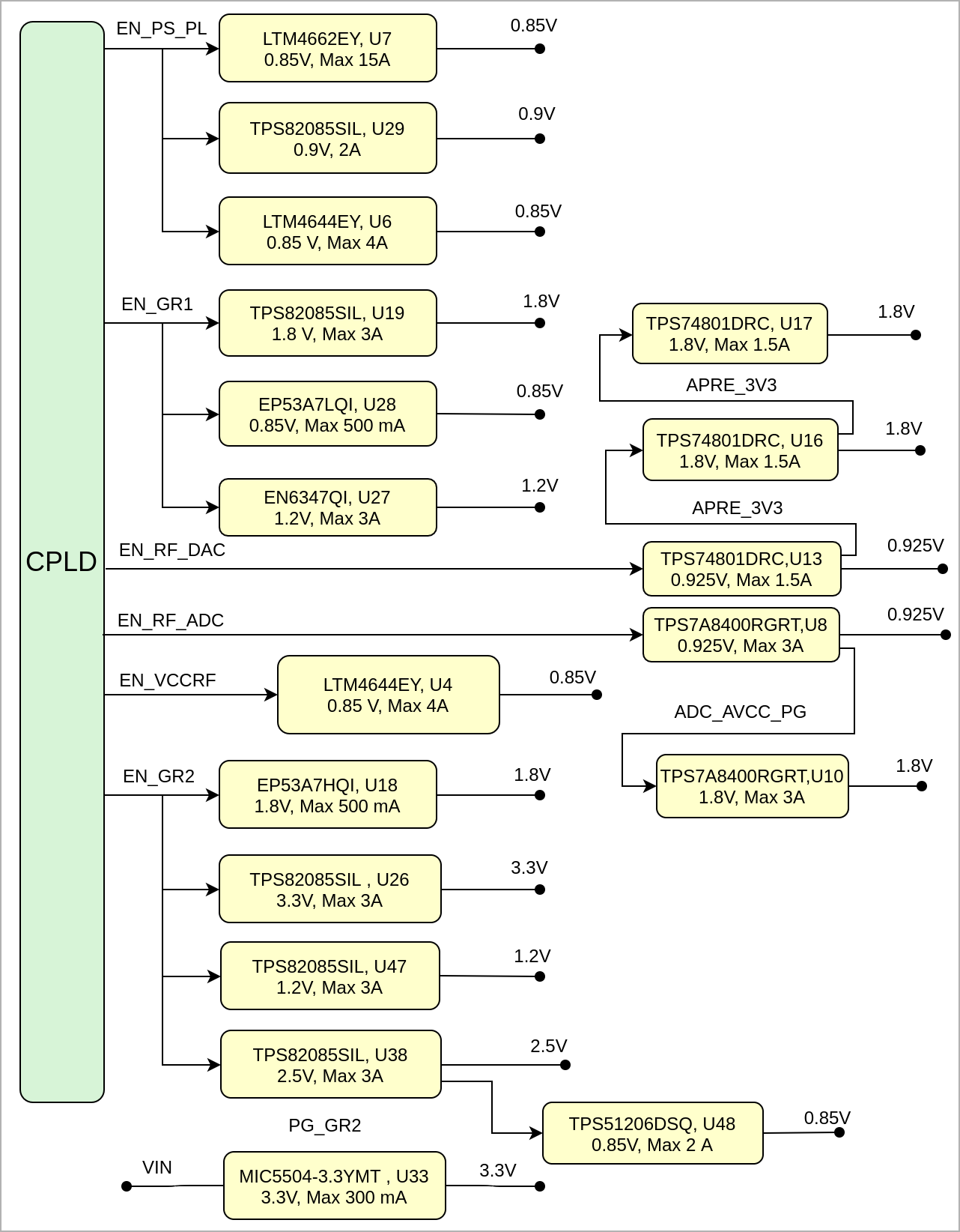
| | EN_PS_PL | Voltage Regulators, U6, U7, U29 | PS/PL Enable Signals | Pulled Down | | EN_GR1 | Voltage Regulators, U19, U27, U28 | MGTAVTT, PSLL | Pulled Down | | EN_GR2 | Voltage Regulators, U38, U18, U38 | PS_MGTRAVTT, 3.3, DDR2.5V | Pulled Down | | EN_RF_ADC | Voltage Regulators, U8 | Enable ADC | Pulled Down | | PG_RF_DAC | Voltage Regulators, U17 | ADC Power Good Status | Pulled Down | | PG_PS_PL | Voltage Regulators, U6, U7, U29 | PS/PL Power Good Status | Pulled Down | | EN_RF_DAC | Voltage Regulators, U13 | Enable DAC | Pulled Down | | PG_RF_DAC | Voltage Regulators, U10 | DAC Power Good Status | Pulled Down |
|
...
The module TE0835 has an EEPROM IC (U23) connected to PSMIO FPGA Bank 501.
...
| Scroll Title |
|---|
| anchor | Table_OBP_CLK |
|---|
| title | Osillators |
|---|
|
| Scroll Table Layout |
|---|
| orientation | portrait |
|---|
| sortDirection | ASC |
|---|
| repeatTableHeaders | default |
|---|
| style | |
|---|
| widths | |
|---|
| sortByColumn | 1 |
|---|
| sortEnabled | false |
|---|
| cellHighlighting | true |
|---|
|
| Designator | Description | Frequency | Note |
|---|
| U14, U21 | MEMS Oscillator | 25MHzU12 |
| | U22 | MEMS Oscillator | 52MHz | 33.33 MHz |
| | Y1 | Crystal Oscillator | 54 MHz |
| | U12 | MEMS Oscillator | 52MHz |
| | U15 | Programmable Clock Generator | U15 | Programmable Clock Generator | Variable |
|
|
Programmable Clock Generator
...
| Scroll Title |
|---|
| anchor | Figure_PWR_PD |
|---|
| title | Power Distribution |
|---|
|
| Scroll Ignore |
|---|
| draw.io Diagram |
|---|
| border | false |
|---|
| viewerToolbar | true |
|---|
| |
|---|
| fitWindow | false |
|---|
| diagramDisplayName | |
|---|
| lbox | true |
|---|
| revision | 1415 |
|---|
| diagramName | TE0835_PWR_PD |
|---|
| simpleViewer | false |
|---|
| width | 639 |
|---|
| links | auto |
|---|
| tbstyle | hidden |
|---|
| diagramWidth | 641 |
|---|
|
|
| Scroll Only |
|---|

|
|
...
| Scroll Title |
|---|
| anchor | Figure_PWR_PS |
|---|
| title | Power Sequency |
|---|
|
| Scroll Ignore |
|---|
| draw.io Diagram |
|---|
| border | false |
|---|
| viewerToolbar | true |
|---|
| |
|---|
| fitWindow | false |
|---|
| diagramDisplayName | |
|---|
| lbox | true |
|---|
| revision | 78 |
|---|
| diagramName | TE0835_PWR_PS |
|---|
| simpleViewer | false |
|---|
| width | 639 |
|---|
| links | auto |
|---|
| tbstyle | hidden |
|---|
| diagramWidth | 641 |
|---|
|
|
| Scroll Only |
|---|
|
|
...
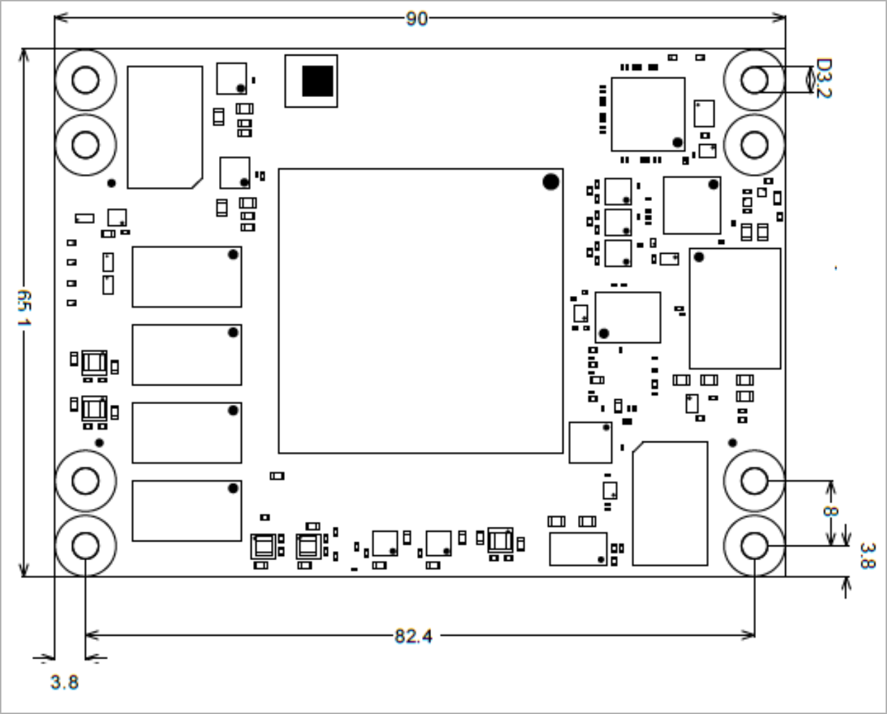
| Scroll Title |
|---|
| anchor | Figure_TS_PD |
|---|
| title | Physical Dimension |
|---|
|
| Scroll Ignore |
|---|
| draw.io Diagram |
|---|
| border | false |
|---|
| viewerToolbar | true |
|---|
| |
|---|
| fitWindow | false |
|---|
| diagramDisplayName | |
|---|
| lbox | true |
|---|
| revision | 34 |
|---|
| diagramName | TE0835_TS_PD |
|---|
| simpleViewer | false |
|---|
| width | 639 |
|---|
| links | auto |
|---|
| tbstyle | hidden |
|---|
| diagramWidth | 640 |
|---|
|
|
| Scroll Only |
|---|
| scroll-pdf | true |
|---|
| scroll-office | true |
|---|
| scroll-chm | true |
|---|
| scroll-docbook | true |
|---|
| scroll-eclipsehelp | true |
|---|
| scroll-epub | true |
|---|
| scroll-html | true |
|---|
| 
|
|
...
| Scroll Title |
|---|
| anchor | Table_RH_HRH |
|---|
| title | Hardware Revision History |
|---|
|
| Scroll Table Layout |
|---|
| orientation | portrait |
|---|
| sortDirection | ASC |
|---|
| repeatTableHeaders | default |
|---|
| style | |
|---|
| widths | |
|---|
| sortByColumn | 1 |
|---|
| sortEnabled | false |
|---|
| cellHighlighting | true |
|---|
|
| Date | Revision | Changes | Documentation Link |
|---|
| 2019-11-05 | REV01 | Initial Release | REV01 |
|
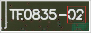
Hardware revision number can be found on the PCB board together with the module model number separated by the dash.
| 2020-06-17 | REV02 | 1. Added a VRP resistor on bank 65; 2. LDO U33 is changed on ADP7102ACPZ; 3. Signal FPGA IO0 is connected on AE18 pin of FPGA; 4. Signal DBG_LED3 is connected on AD18 pin of FPGA; 5. Signal MIO13_25 connected to J1 pin 33 instead MIO25. 6. Resistor R84 is removed; 7. LED D1 moved on edge of PCB; 8. Added THT testpoints J4 on CPLD_JTAGEN, R76 was removed; 9. Signals B49_XX_X are renamed in B88_XX_X; 10. C241 is changed on 1nF; 11. Length of CLK signals on RFADC and RFDAC are adjusted; 12. Wrong connection on U8 is fixed (PCB); 13. Wrong connection PGOOD1 pin of U7 is fixed; 14. R17 is changed from 35,5K to 33K for VCC_PL_PS correction. | REV02 |
|
Hardware revision number can be found on the PCB board together with the module model number separated by the dash.
| Scroll Title |
|---|
| anchor | Figure_RV_HRN |
|---|
| title | Board hardware revision number. |
|---|
|
|
| Scroll Title |
|---|
| anchor | Figure_RV_HRN |
|---|
| title | Board hardware revision number. |
|---|
|
| scroll-ignore |
|---|
| draw.io Diagram |
|---|
| border | false |
|---|
| viewerToolbar | true |
|---|
| |
|---|
| fitWindow | false |
|---|
| diagramDisplayName | |
|---|
| lbox | true |
|---|
| revision | 46 |
|---|
| diagramName | TE0835_RV_HRN |
|---|
| simpleViewer | false |
|---|
| width | 200 |
|---|
| links | auto |
|---|
| tbstyle | hidden |
|---|
| diagramWidth | 198 |
|---|
|
|
| Scroll Only |
|---|
|
|
...
| Scroll Title |
|---|
| anchor | Table_RH_DCH |
|---|
| title | Document change history. |
|---|
|
| Scroll Table Layout |
|---|
| orientation | portrait |
|---|
| sortDirection | ASC |
|---|
| repeatTableHeaders | default |
|---|
| style | |
|---|
| widths | |
|---|
| sortByColumn | 1 |
|---|
| sortEnabled | false |
|---|
| cellHighlighting | true |
|---|
|
| Date | Revision | Contributor | Description |
|---|
| Page info |
|---|
| infoType | Modified date |
|---|
| dateFormat | yyyy-MM-dd |
|---|
| type | Flat |
|---|
|
| | Page info |
|---|
| infoType | Current version |
|---|
| prefix | v. |
|---|
| type | Flat |
|---|
| showVersions | false |
|---|
|
| | Page info |
|---|
| infoType | Modified by |
|---|
| type | Flat |
|---|
| showVersions | false |
|---|
|
| | -- | all | | Page info |
|---|
| infoType | Modified users |
|---|
| type | Flat |
|---|
| showVersions | false |
|---|
|
| |
|
...
| Include Page |
|---|
| IN:Legal Notices |
|---|
| IN:Legal Notices |
|---|
|
| draw.io Diagram |
|---|
| border | false |
|---|
| viewerToolbar | true |
|---|
| |
|---|
| fitWindow | false |
|---|
| diagramDisplayName | |
|---|
| lbox | true |
|---|
| revision | 17 |
|---|
| diagramName | TE0835_OV_MC |
|---|
| simpleViewer | false |
|---|
| width | 639 |
|---|
| links | auto |
|---|
| tbstyle | hidden |
|---|
| diagramWidth | 641 |
|---|
|