...
| Page properties |
|---|
|
Important General Note: |
...
...
| Scroll Title |
|---|
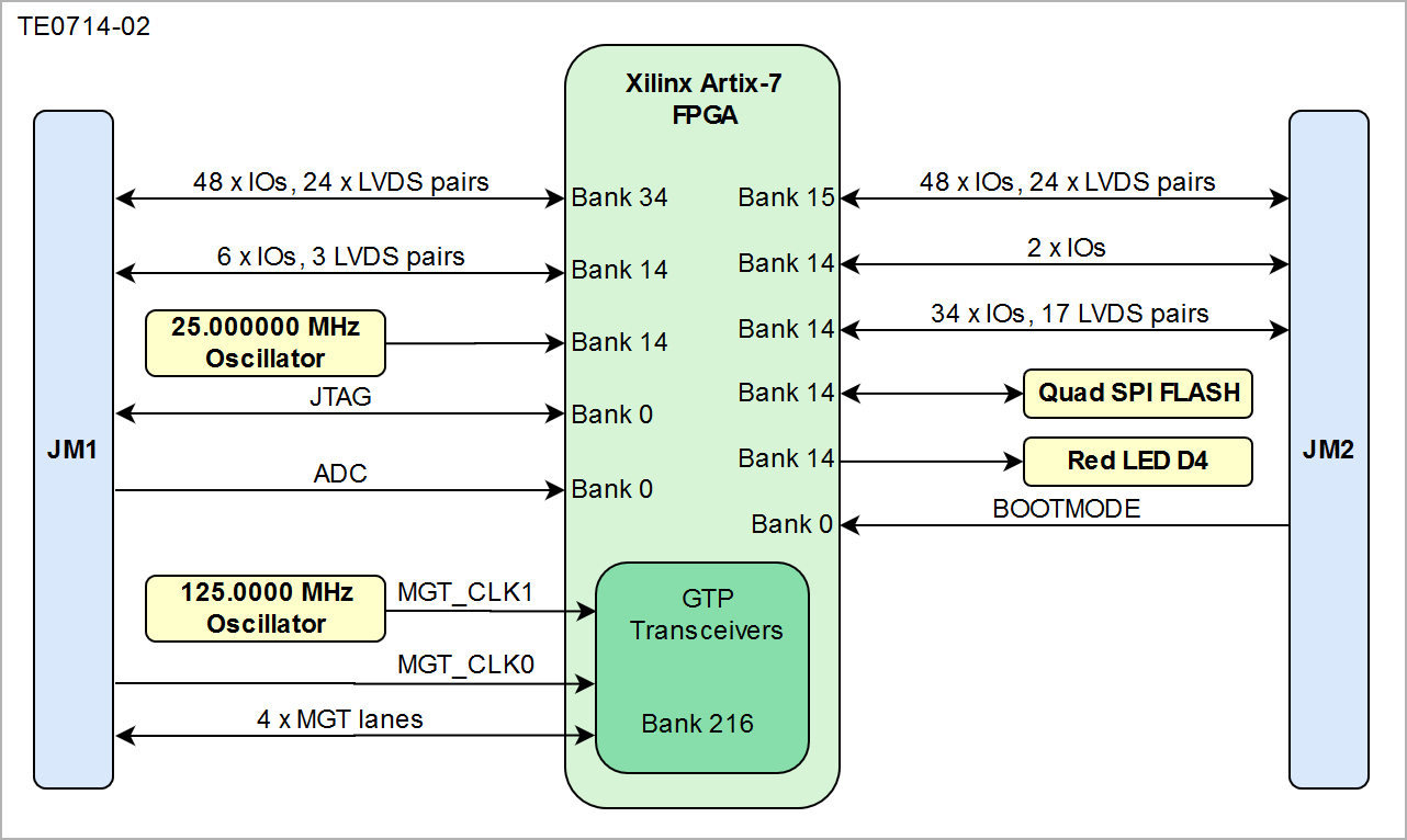
| anchor | Figure_OV_BD |
|---|
| title | TE0714 block diagram |
|---|
|
| Scroll Ignore |
|---|
| draw.io Diagram |
|---|
| border | false |
|---|
| viewerToolbar | true |
|---|
| |
|---|
| fitWindow | false | diagramDisplayName |
|---|
| lbox | true |
|---|
| revision | 4 |
|---|
| diagramName | BD-TE0714-02 |
|---|
| simpleViewer | true | width |
|---|
| links | auto |
|---|
| tbstyle | top |
|---|
| lbox | true |
|---|
| diagramWidth | 641 |
|---|
| revision | 4 |
|---|
|
|
| Scroll Only |
|---|
|
|
Main Components
...
| Scroll Title |
|---|
| anchor | Figure_OV_MC |
|---|
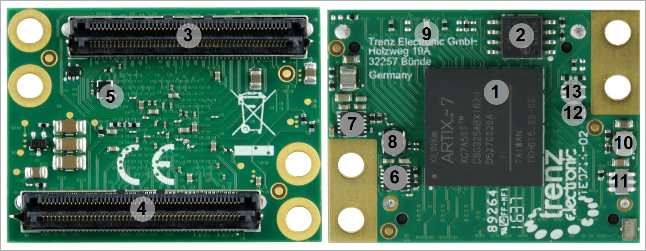
| title | TE0714 main components |
|---|
|
| Scroll Ignore |
|---|
| draw.io Diagram |
|---|
| border | false |
|---|
| viewerToolbar | true |
|---|
| |
|---|
| fitWindow | false | diagramDisplayName |
|---|
| lbox | true |
|---|
| revision | 2 |
|---|
| diagramName | MC-TE0714 |
|---|
| simpleViewer | true | width |
|---|
| links | auto |
|---|
| tbstyle | top |
|---|
| lbox | true |
|---|
| diagramWidth | 641 |
|---|
| revision | 2 |
|---|
|
|
| Scroll Only |
|---|
|
|
- Xilinx Artix-7 FPGA (XC7A series), U4
- 16 MByte SPI Flash, U7
- B2B connector Samtec Razor Beam™ LSHM-150, JM2
- B2B connector Samtec Razor Beam™ LSHM-150, JM1
- 25 MHz oscillator, U8
- Single output low-dropout linear regulator (1.2V_MGT), U6
- Single output low-dropout linear regulator (1.0V_MGT), U5
- Low-jitter precision LVDS 125 MHz oscillator (GT Clock), U2
- Red indication LED, D4
- Step-down DC-DC converter (1.0V), U1
- PFET load switch with configurable slew rate (3.3V), Q1
- Low-power step-down DC-DC converter (1.8V), U3
- Voltage detector for circuit initialization and timing supervision, U23
...
Initial Delivery State
| Scroll Title |
|---|
| anchor | Table_OV_IDS |
|---|
| title | Initial delivery state of programmable devices on the module. |
|---|
|
| Scroll Table Layout |
|---|
| orientation | portrait |
|---|
| sortDirection | ASC |
|---|
| repeatTableHeaders | default | style |
|---|
| widths | 30%,25%,45% |
|---|
| sortByColumn | 1 |
|---|
| sortEnabled | false |
|---|
| cellHighlighting | true |
|---|
|
Storage device name | Content | Notes |
|---|
SPI Flash OTP Area | Empty, not programmed | Except serial number programmed by flash vendor | SPI Flash Quad Enable bit | Programmed |
| SPI Flash main array | demo design |
| eFUSE USER | Not programmed |
| eFUSE Security | Not programmed |
|
|
Control Signals
| Page properties |
|---|
|
- Overview of Boot Mode, Reset, Enables,
|
Boot process is controlled by signals on the board to board (B2B) connector.
| Scroll Title |
|---|
| anchor | Table_OV_BS |
|---|
| title | Boot signals. |
|---|
|
| Scroll Table Layout |
|---|
| orientation | portrait |
|---|
| sortDirection | ASC |
|---|
| repeatTableHeaders | default | style |
|---|
| widths | 16%,14%,19%,51 |
|---|
| sortByColumn | 1 |
|---|
| sortEnabled | false |
|---|
| cellHighlighting | true |
|---|
|
| Signal | Direction | Signal State | Description |
|---|
BOOTMODE
| input | high or open | Master SPI, x4 Mode
| low or ground
| Slave SelectMAP | | PROG_B | input | pulsed low | Clear FPGA configuration (falling edge) and initiate a new configuration sequenz (next rising edge). | | DONE | output | high | Completion of configuration sequence. |
|
| Note |
|---|
SPI FPGA pins D02 and D03 have no pull-ups on the module, so with PUDC=High option, those pins are floating if there are no pull-ups on baseboard. As those pins have SPI RESET function when Quad mode is not enabled, it is mandatory to either add pull-ups on user baseboard or program the Quad Enable bit in Flash nonvolatile status register. |
...
| Scroll Title |
|---|
| anchor | Table_SIP_JTAG |
|---|
| title | JTAG signals. |
|---|
|
| Scroll Table Layout |
|---|
| orientation | portrait |
|---|
| sortDirection | ASC |
|---|
| repeatTableHeaders | default |
|---|
| stylesortByColumnwidths | 1 |
|---|
| sortByColumn | 1 |
|---|
| sortEnabled | false |
|---|
| cellHighlighting | true |
|---|
|
Signal Name | B2B Pin |
|---|
| TCK | JM1:89 | | TDI | JM1:85 | | TDO | JM1:87 | | TMS | JM1:91 |
|
...
| Scroll Title |
|---|
| anchor | Table_SIP_B2B |
|---|
| title | B2B I/Os |
|---|
|
| Scroll Table Layout |
|---|
| orientation | portrait |
|---|
| sortDirection | ASC |
|---|
| repeatTableHeaders | default | style |
|---|
| widths | sortByColumn | 1 |
|---|
| sortEnabled | false |
|---|
| cellHighlighting | true |
|---|
|
| FPGA Bank | B2B Connector | I/O Signal Count | Voltage Level | Notes |
|---|
| 14 | JM1 | 6 | VCCIO_0 |
| | 14 | JM2 | 36 | VCCIO_0 | NB! 17 LVDS pairs possible. | | 15 | JM2 | 48 | VCCIO15 | Supplied by the baseboard. | | 34 | JM1 | 48 | VCCIO34 | Supplied by the baseboard. | | 216 | JM1 | 16 | MGT_AVCC MGT_AVTT | 4 x GTP lanes. |
|
...
| Scroll Title |
|---|
| anchor | Table_OBP_LEDs |
|---|
| title | LED connection. |
|---|
|
| Scroll Table Layout |
|---|
| orientation | portrait |
|---|
| sortDirection | ASC |
|---|
| repeatTableHeaders | default | style |
|---|
| widths | sortByColumn | 1 |
|---|
| sortEnabled | false |
|---|
| cellHighlighting | true |
|---|
|
LED | Color | FPGA | Notes |
|---|
D4 | Red | K18 | User programmable |
|
...
| Scroll Title |
|---|
| anchor | Table_OBP_Clocks |
|---|
| title | Clock signals. |
|---|
|
| Scroll Table Layout |
|---|
| orientation | portrait |
|---|
| sortDirection | ASC |
|---|
| repeatTableHeaders | default | style |
|---|
| widths | 14%,15%,6%,9%,56% |
|---|
| sortByColumn | 1 |
|---|
| sortEnabled | false |
|---|
| cellHighlighting | true |
|---|
|
Clock | Default Frequency | IC | FPGA | Notes |
|---|
| CLK25MHz | 25 MHz | U8 | T14 | Frequency depends on the module variant. Output is compatible to 3.3V and 1.8V I/O standard of the FPGA bank. | | MGT_CLK | 125MHz | U2 | B6/B5 | Frequency depends on the module variant |
|
...
| Scroll Title |
|---|
| anchor | Table_PWR_PC |
|---|
| title | Power Consumption |
|---|
|
| Scroll Table Layout |
|---|
| orientation | portrait |
|---|
| sortDirection | ASC |
|---|
| repeatTableHeaders | default | style | widths |
|---|
| sortByColumn | 1 |
|---|
| sortEnabled | false |
|---|
| cellHighlighting | true |
|---|
|
| Test Condition (25 °C ambient) | VIN Current mA | Notes |
|---|
| TE0714-35, TEBT0714, empty design, GT not enabled | 110mA |
|
|
...
| Scroll Title |
|---|
| anchor | Figure_PWR_PD |
|---|
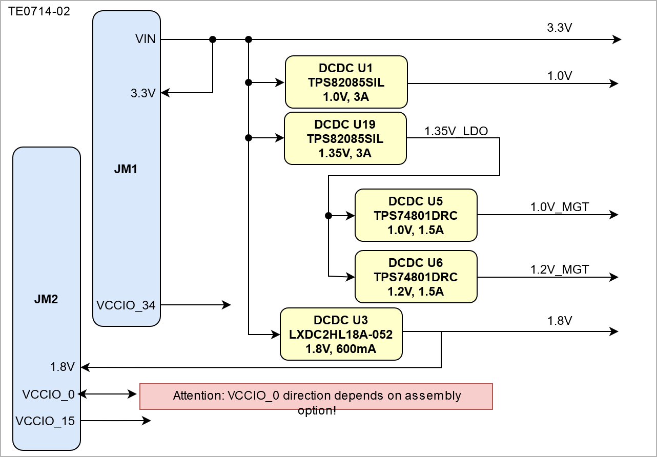
| title | Power Distribution |
|---|
|
| Scroll Ignore |
|---|
| draw.io Diagram |
|---|
| border | false |
|---|
| viewerToolbar | true |
|---|
| |
|---|
| fitWindow | false | diagramDisplayName |
|---|
| lbox | true |
|---|
| revision | 6 |
|---|
| diagramName | PD-TE0714 |
|---|
| simpleViewer | true | width |
|---|
| links | auto |
|---|
| tbstyle | top |
|---|
| lbox | true |
|---|
| diagramWidth | 641 |
|---|
| revision | 10 |
|---|
|
|
| Scroll Only |
|---|
|
|
Power-On Sequence
...
| Scroll Title |
|---|
| anchor | Figure_PWR_PS |
|---|
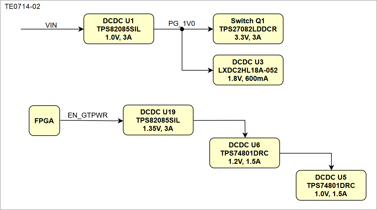
| title | Power-On Sequency |
|---|
|
| Scroll Ignore |
|---|
| draw.io Diagram |
|---|
| border | false |
|---|
| viewerToolbar | true |
|---|
| |
|---|
| fitWindow | false | diagramDisplayName |
|---|
| lbox | true |
|---|
| revision | 2 |
|---|
| diagramName | TE0714-02_Power_Sequenz |
|---|
| simpleViewer | true | width |
|---|
| links | auto |
|---|
| tbstyle | top |
|---|
| lbox | true |
|---|
| diagramWidth | 641 |
|---|
| revision | 2 |
|---|
|
|
| Scroll Only |
|---|
|
|
Power Rails
| Scroll Title |
|---|
| anchor | Table_PWR_PR |
|---|
| title | Power Rails |
|---|
|
| Scroll Table Layout |
|---|
| orientation | portrait |
|---|
| sortDirection | ASC |
|---|
| repeatTableHeaders | default | style |
|---|
| widths | sortByColumn | 1 |
|---|
| sortEnabled | false |
|---|
| cellHighlighting | true |
|---|
|
| | | Direction | Note |
|---|
| VIN | 98, 100 | - | input | supply voltage | | VCCIO_0 | - | 54 | input | high range bank voltage | | VCCIO_15 | - | 53 | input | high range bank voltage | | VCCIO_34 | 62 | - | input | high range bank voltage | | 3.3V | 84 | - | output | internal 3.3V voltage level | | 1.8V | - | 17 | output | internal 1.8V voltage level |
|
...
| Scroll Title |
|---|
| anchor | Table_PWR_BV |
|---|
| title | Bank Voltages |
|---|
|
| Scroll Table Layout |
|---|
| orientation | portrait |
|---|
| sortDirection | ASC |
|---|
| repeatTableHeaders | default |
|---|
| stylesortByColumnwidths | 1 |
|---|
| sortByColumn | 1 |
|---|
| sortEnabled | false |
|---|
| cellHighlighting | true |
|---|
|
| | |
|---|
0 Config and B14 | 1.8V or 3.3V | Depends on module assembly variant. See R21, R22 and R27 assembly option* | 15 | User | Supplied from baseboard via B2B connector, max 3.3V | 34 | User | Supplied from baseboard via B2B connector, max 3.3V |
|
Board to Board Connectors
- *R21 assembled: 3.3V and B2B is output if R27 is assembled
- *R22 assembled 1.8V and B2B is output if R27 is assembled
- *R21 and R22 not assembled , B2B is input and carrier defines voltage → pay attention on assembled flash!
|
Board to Board Connectors
| Page properties |
|---|
|
- This section is optional and only for modules.
- use "include page" macro and link to the
|
| Page properties |
|---|
|
- This section is optional and only for modules.
- use "include page" macro and link to the general B2B connector page of the module series, for example: 4 x 5 SoM LSHM B2B Connectors
|
...
| Scroll Title |
|---|
| anchor | Table_TS_AMR |
|---|
| title | Module absolute maximum ratings. |
|---|
|
| Scroll Table Layout |
|---|
| orientation | portrait |
|---|
| sortDirection | ASC |
|---|
| repeatTableHeaders | default |
|---|
| stylesortByColumn | widths | sortByColumn1 | 1 |
|---|
| sortEnabled | false |
|---|
| cellHighlighting | true |
|---|
|
| Parameter | Min | Max | Units | Reference Document |
|---|
VIN supply voltage | -0.1 | 6.0 | V | - | | HR I/O banks supply voltage (VCCO) | -0.5 | 3.6 | V | Xilinx datasheet DS181 | | HR I/O banks input voltage | -0.4 | VCCO + 0.55 | V | Xilinx datasheet DS181 | | GTP transceivers Tx/Rx input voltage | -0.5 | 1.26 | V | Xilinx datasheet DS181 | Voltage on module JTAG pins | -0.4 | VCCO_0 + 0.55 | V | Xilinx datasheet DS181 | Storage temperature | -40 | +85100 | °C | - |
|
Recommended Operating Conditions
Recommended Operating Conditions
| Table_TS_ROC | | title | Recommended Operating Conditions |
|---|
|
| Scroll Title |
|---|
| anchor | Table_TS_ROC |
|---|
| title | Recommended Operating Conditions |
|---|
|
This TRM is generic for all variants. Variants of modules are described here: Article Number Information Modules with commercial temperature grade are equipped with components that cover at least the range of 0°C to 75°C Modules with extended temperature grade are equipped with components that cover at least the range of 0°C to 85°C Modules with industrial temperature grade are equipped with components that cover at least the range of -40°C to 85°C The actual operating temperature range will depend on the FPGA / SoC design / usage and cooling and other variables. |
| Scroll Table Layout |
|---|
| orientation | portrait |
|---|
| sortDirection | ASC |
|---|
| repeatTableHeaders | default | style |
|---|
| widths | sortByColumn | 1 |
|---|
| sortEnabled | false |
|---|
| cellHighlighting | true |
|---|
|
| Parameter | Min | Max | Units | Reference Document |
|---|
| VIN supply voltage | 3.135 | 3.45 | V | - | | HR I/O banks supply voltage (VCCO) | 1.14 | 3.465 | V | Xilinx datasheet DS181 | | HR I/O banks input voltage | -0.20 | VCCO + 0.2020V | V | Xilinx datasheet DS181 | | Voltage on module JTAG pins | 3.135 | 0 | VCCO_0 + 5%3.465 | V | Xilinx datasheet DS181 |
|
Physical Dimensions
...
| Scroll Title |
|---|
| anchor | Table_VCP_SO |
|---|
| title | Trenz Electronic Shop Overview |
|---|
|
| Scroll Table Layout |
|---|
| orientation | portrait |
|---|
| sortDirection | ASC |
|---|
| repeatTableHeaders | default | style | widths |
|---|
| sortByColumn | 1 |
|---|
| sortEnabled | false |
|---|
| cellHighlighting | true |
|---|
|
|
...
| Scroll Title |
|---|
| anchor | Table_RH_HRH |
|---|
| title | Hardware Revision History |
|---|
|
| Scroll Table Layout |
|---|
| orientation | portrait |
|---|
| sortDirection | ASC |
|---|
| repeatTableHeaders | default | stylewidths | default |
|---|
| sortByColumn | 1 |
|---|
| sortEnabled | false |
|---|
| cellHighlighting | true |
|---|
|
|
...
| Scroll Title |
|---|
| anchor | Table_RH_DCH |
|---|
| title | Document change history |
|---|
|
| Scroll Table Layout |
|---|
| orientation | portrait |
|---|
| sortDirection | ASC |
|---|
| repeatTableHeaders | default | style |
|---|
| widths | sortByColumn | 1 |
|---|
| sortEnabled | false |
|---|
| cellHighlighting | true |
|---|
|
Date | Revision | Authors | Description |
|---|
| Page info |
|---|
| modified-date |
|---|
| modified-date |
|---|
| dateFormat | yyyy-MM-dd |
|---|
|
| | Page info |
|---|
| infoType | Current version |
|---|
| prefix | v. |
|---|
| type | Flat |
|---|
| showVersions | false |
|---|
|
| | Flat | | showVersions | false |
|---|
| Page info |
|---|
| infoType | Modified by |
|---|
| type | Flat |
|---|
| showVersions | false |
|---|
|
| | - Updated storage temperatur.
| | 2021-04-07 | v59 | Thomas Steffens | - changed operating conditions
| | 2019-03-04 | v55 | John Hartfiel | - Restore and modify v.50
- Correction max IO count on key features
- Change history table
- typo correction
| | 2019-01-07 | v.50 | John Hartfiel | - Updated to TRM version 2.2
- Style modifications
| | Sept 2018 | v.48 | Martin Rohrmüller | - Updated to TRM version 2.1
- Updated B2B Connectors
- Style modifications
| | 2018-09-17 | v.38 | Martin Rohrmüller | - Added power rail section
- Added Rev 02 Flash PCN
- Corrected table headings
| | 2018-09-17 | v.36 | Martin Rohrmüller | | | 2018-04-04 | | Martin Rohrmüller | Corrected clock net designator in table. | | 2017-05-28 | | Jan Kumann | - Board-to-Board I/O section added.
- New physical dimensions images.
- Documents sections rearranged.
| | 2017-03-20 | | John Hartfiel | - Notes on Clocking section.
| | 2017-01-27 | v.25 | Jan Kumann | | | 2016-12-01 | | Jan Kumann | - Changes in the document structure, few corrections.
| | 2016-11-18 | v.14
| Thorsten Trenz, Emmanuel Vassilakis | - Hardware revision 02 specific changes.
| 2016-06-01 | | | | | -- | all | | Page info |
|---|
| infoType | Modified users |
|---|
| type | Flat |
|---|
| showVersions | false |
|---|
|
| -- |
|
Disclaimer
| Include Page |
|---|
| IN:Legal Notices |
|---|
| IN:Legal Notices |
|---|
|
...