VG96 connector (mounting holes and solder pads, J6) and 50-pin IDC male connector socket (J5) for access to PL I/O-bank pins
USB2.0 type A connector, or optionally Micro USB 2.0 connector
1 x RJ45 GbE MagJack (J3), connected via MDI to B2B connector JB1
1 x Marvell Alaska 88E1512 GbE PHY, providing Ethernet interface in conjunction with RJ45 GbE MagJack (J2)
4 A High-Efficiency Power SoC DC-DC Step-Down Converter (Enpirion EN6347) for 3.3V power supply
XMOD JTAG- / UART-header JX1
Micro SD card socket
SDIO port expander with voltage-level translation and jumper (J13) for selection of SDIO voltage on SoM side
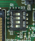
DIP-switches S1 to set SoM's control signals
1 x user-push button (S2), by default configured as system reset button
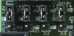
3 x VCCIO selection jumper J10, J11 and J12 to set SoM's PL I/O-bank voltages
5V power supply barrel jack
...
VCCIO voltage selection jumpers are all set to 1.8 V.
S2 switch configured as reset button.
One VG96 connector (not soldered to the board, but included in the package as separate component)
Different delivery configurations are available upon request.
...
Scroll Title
anchor
Table_SIP_XMODconfig
title
XMOD adapter board DIP-switch positions for voltage configuration
Scroll Table Layout
orientation
portrait
sortDirection
ASC
repeatTableHeaders
default
style
widths
sortByColumn
1
sortEnabled
false
cellHighlighting
true
XMOD DIP-switches
Position
Switch 1
ON
Switch 2
OFF
Switch 3
OFF
Switch 4
ON
Note
Use Xilinx AMD compatible TE0790 adapter board (designation TE-0790-xx with out 'L') to program the Xilinx AMD Zynq devices.
The TE0790 adapter board's CPLD have to be configured with the Standard variant of the firmware. Refer to the TE0790 Resources Site for further information and firmware download.
...
The SD Socket is routed to the on-board Texas Instruments TXS02612 SDIO port expander U4. This IC provides a necessary VDD/VCCIO translation between the MicroSD Card socket J4 (3.3V) and the SoM's Zynq device MIO-bank (1.8V/3.3V depending on Module, compare jumper J13):
Scroll Title
anchor
Table_SIP_SD
title
SD IO interface signals
Scroll Table Layout
orientation
portrait
sortDirection
ASC
repeatTableHeaders
default
style
widths
sortByColumn
1
sortEnabled
false
cellHighlighting
true
SD IO Signal Schematic Name
Connected to
Note
eSD_DAT0
U4-18
SD IO data
eSD_DAT1
U4-16
SD IO data
eSD_DAT2
U4-23
SD IO data
eSD_DAT3
U4-22
SD IO data
eSD_CLK
U4-19
SD IO clock
eSD_CMD
U4-20
SD IO command
MIO0
J5-29
Card Detect signal
...
Scroll Title
anchor
Table_OBP_DIP
title
DIP-switch SoM configuration settings
Scroll Table Layout
orientation
portrait
sortDirection
ASC
repeatTableHeaders
default
style
widths
sortByColumn
1
sortEnabled
false
cellHighlighting
true
Switch
Signal Name
ON
OFF
Notes
S1-1
-
-
-
Not connected.
S1-2
PROGMODE
JTAG enabled for programing mounted SoM's Zynq-SoC.
JTAG enabled for programing mounted SoM's SC-CPLD.
-
S1-3
MODE
Drive SoM SC CPLD pin 'MODE' low. (SD-Boot)
Leave SoM SC CPLD pin 'MODE' open. (QSPI-Boot)
Boot mode configuration, if supported by SoM. (Depends also on SoM's SC-CPLD firmware).
S1-4
EN1
Drive SoM SC CPLD pin 'EN1' low.
Drive SoM SC CPLD pin 'EN1' high.
Usually used to enable/disable FPGA core-voltage supply. (Depends also on SoM's SC CPLD firmware).
Note: Power-on sequence will be intermitted if S1-4 is set to OFF and if functionality is supported by SoM.
Note
Note: Compared to the former revision 02 of this board, the DIP-switch is rotated by 180° due to routing issues.
Scroll Title
anchor
Figure_OBP_DIP
title
User DIP-switch S1
VCC Selection
...
Jumpers
Note
Note: The corresponding PL I/O-bank supply-voltages of the 4 x 5 SoM to the selectable base-board voltages VCCIOA, VCCIOB and VCCIOC are depending on the mounted 4 x 5 SoM and varying in order of the used model.
Refer to the SoM's schematic for information about the specific pin assignments on module's B2B-connectors regarding the PL I/O-bank supply-voltages and to the 4 x 5 Module integration Guide for VCCIO voltage options.
The Carrier Board's push button S2 is connected to the 'RESIN' signal, the function of the button is to trigger a reset of the mounted SoM by driving the reset-signal 'RESIN' to ground.
Gigabit Ethernet PHY
The TE0706 Carrier Board is equipped with a Marvell Alaska 88E1512 Gigabit Ethernet PHY (U6), which provides in conjunction with the Gigabit Ethernet MagJack J2 a 1000Base-T Ethernet (GbE) interface. The Ethernet PHY RGMII interface is connected to the B2B connector JB3, where they can be accessed by the mounted SoM's PS bank. The I/O Voltage is fixed at 1.8V. Reference clock input of the PHY is supplied from the on-board 25.000000 MHz oscillator (U7), the 125MHz output clock signal *CLK125' is connected to the B2B connector pin JB3-32.
Scroll Title
anchor
Table_SIP_ETH
title
RJ45 connectors
Scroll Table Layout
orientation
portrait
sortDirection
ASC
repeatTableHeaders
default
style
widths
sortByColumn
1
sortEnabled
false
cellHighlighting
true
PHY U6 pins
B2B-pin
Notes
ETH-MDC/ETH-MDIO
JB3-49, JB3-51
-
PHY_LED0
-
Connected to GbE MagJack J2 LED0 (green). Also connected to J5-24 (PHY_LED0_CON).
PHY_LED1
-
Connected to GbE MagJack J2 LED1 (green). Also connected to J5-23 (PHY_LED1_CON).
PHY_INT
JB3-33
-
CONFIG
JB3-60
-
CLK125
JB3-32
PHY Clock (125 MHz) output.
ETH-RST
JB3-53
-
RGMII
JB3-31 JB3-37 - JB-44, JB3-47, JB3-57 - JB-59
Reduced Gigabit Media Independent Interface.
12 pins.
SGMII
Note
ETH-RXCK is connected via 0Ohm to JB3-31 (R18)and JB3-58 (R19). Usage depends on Module and AMD IP restrictions In case of performance problems remove 0Ohm resistor from the unused Pin.
The TE0706 Carrier Board is equipped with a Texas Instruments TXS02612 SDIO SDIO Port Expander, which is needed for voltage translation due to different voltage levels of the Micro SD Card and the PS MIO-bank of the Zynq device of the mounted SoM. The Micro SD Card has 3.3V signal voltage level, but the PS MIO-bank on the Xilinx AMD Zynq module has VCCIO of 1.8V or 3.3V depending on the attached module. this This has to beselected be selected by J13.
Scroll Title
anchor
Table_OBP_SDIO
title
SDIO Port Expander
Scroll Table Layout
orientation
portrait
sortDirection
ASC
repeatTableHeaders
default
style
widths
sortByColumn
1
sortEnabled
false
cellHighlighting
true
SD-Card Signal Schematic Name
SD-Card Connected to
Connected to
SD IO Signal Schematic Name
B2B
Note
eSD_DAT0
U4-18
U4-6
SD_DAT0
JB1-24
SD IO data
eSD_DAT1
U4-16
U4-7
SD_DAT1
JB1-22
SD IO data
eSD_DAT2
U4-23
U4-1
SD_DAT2
JB1-20
SD IO data
eSD_DAT3
U4-22
U4-3
SD_DAT3
JB1-18
SD IO data
eSD_CLK
U4-19
U4-9
SD_CLK
JB1-28
SD IO clock
eSD_CMD
U4-20
U4-4
SD_CMD
JB1-26
SD IO command
MIO0
-
-
-
JB1-88
Card Detect signal
...
The maximum power consumption of the Carrier Board depends mainly on the mounted SoM's FPGA design running on the Zynq device.
Xilinx AMD provide a power estimator excel sheets to calculate power consumption. It's also possible to evaluate the power consumption of the developed design with Vivado. See also Trenz Electronic Wiki FAQ.
...
Scroll Title
anchor
Figure_TS_PD
title
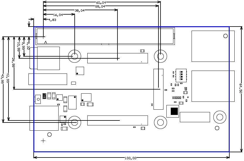
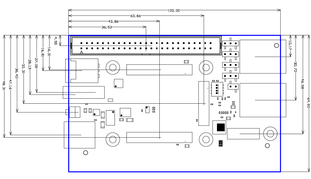
Physical Dimension
Scroll Ignore
Image Removed
draw.io Diagram
...
border
details
true
hidden
viewerToolbar
true
fitWindow
false
id
Comments
diagramName
AD_TE0706-03
simpleViewer
false
width
diagramWidth
627
revision
3
Scroll Only
Image Added
Currently Offered Variants
Page properties
hidden
true
id
Comments
Set correct link to the shop page overview Set correct link to the shop page overview table of the product on English and German.