Page History
...
Block Diagram
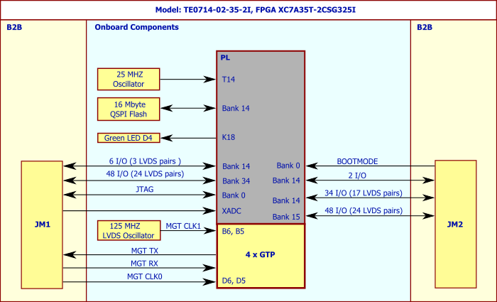
Main Components
...
...
...
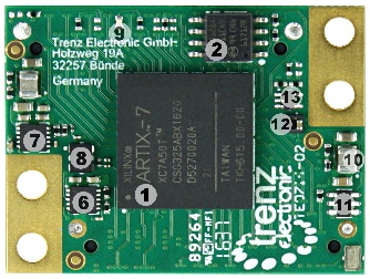
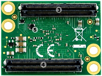
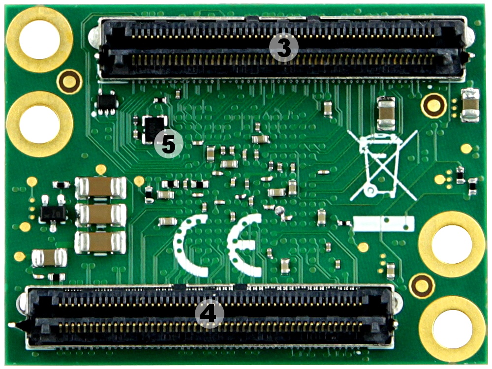
Top view
...
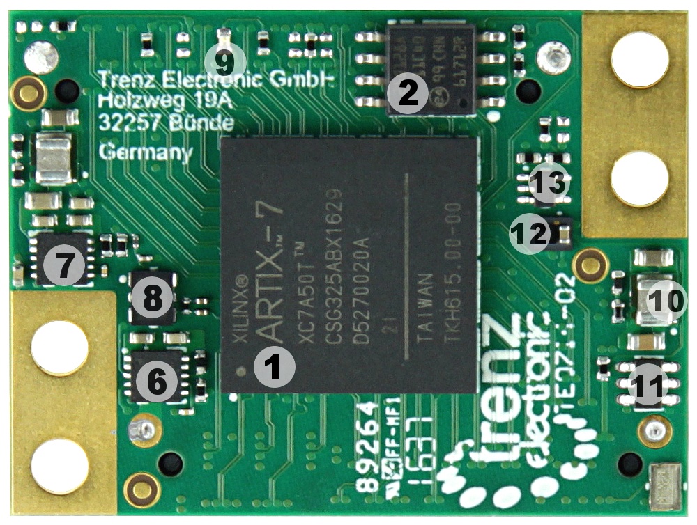
- Xilinx Artix-7 FPGA (XC7A series), U4
- SPI Flash, U7
- B2B Connector, JM2
- B2B Connector, JM1
- MEMS Oscillator (PL Clock), U8
- Single Output Low-Dropout Linear Regulator , U6 (1.2V_MGT), U6
- Single Output Low-Dropout Linear Regulator , U5 (1.0V_MGT), U5
- Low-Jitter Precision LVDS Oscillator (GT Clock), U2
- Red Indication LED, D4
- Step-Down DC-DC Converter , U1 (1.0V), U1
- PFET Load Switch With Configurable Slew Rate , Q1 (3.3V), Q1
- Low Power Step-Down DC-DC Converter , U3 (1.8V), U3
- Voltage Detector for Circuit Initialization and Timing Supervision, U23
Key Features
Xilinx Artix-7 FPGA (A15T, A35T, A50T)
- Rugged for Sock and High Vibration
- 16 MByte QSPI Flash Memory
- Differential MEMS Oscillator for GT Clocking
- MEMS Oscillator for PL Clocks (Optional)
- Plug-On Module With 2 × 100-Pin High-Speed Hermaphroditic Strips
- 144 FPGA I/O's (Max 68 Differential)
- XADC Analog Input
- 4 GTP (High-Performance Transceiver) Lanes
- GT Reference Clock Input
- Optimized I/O and Power Pins for Good Signal Integrity
- On-board High-Efficiency DC-DC Converters
- Power Supply for All On-Board Components
- eFUSE Bit-Stream Encryption (AES)
- One User Configurable LED
Different configurations for cost and performance optimization available upon request. Available options are:
- FPGA Type (A15T, A35T, A50T), temperature grade
- GT Clock Frequency (or none if not implemented)
- PL Clock Frequency and precision (or none if not implemented)
- Config and B14 Bank Voltage: 1.8V or 3.3V
- SPI Flash type (or none if not implemented)
- LED Color (or none if not implemented)
- PUDC Pin strapping (pull high or pull down)
- GT Power Enable pin strapping (default power enabled or disabled)
Initial Delivery State
Storage device name | Content | Notes |
|---|---|---|
SPI Flash OTP Area | Empty, not programmed | Except serial number programmed by flash vendor |
SPI Flash Quad Enable bit | Programmed | |
SPI Flash main array | demo design | |
EFUSE eFUSE USER | Not programmed | |
EFUSE eFUSE Security | Not programmed |
Signals, Interfaces and Pins
...
| PCB Revision | Changes | PCN link | Documentation link |
|---|---|---|---|
| 02 | VCCIO0 added to B2B | PCN-20160815 | TE0714 |
01 | Current Hardware Revision, no changes - | - | TE0714-01 TRM |
Hardware revision number is printed on the PCB board next to the module model number separated by the dash.
...
Document Change History
Date | Revisionvision | Authors | Description | |
|---|---|---|---|---|
| 2016-12-01 | Jan Kumann | Changes in the document structure, few corrections. | ||
| 2016-11-18 | V.14
| V14 | Antti Lukats, Thorsten Trenz, Emmanuel Vassilakis | Hardware revision 02 specific changes.Changes for REV 02 |
2016-06-01 | V9 | Antti LukatsV.9 | Initial version. |
Disclaimer
| Include Page | ||||
|---|---|---|---|---|
|
Overview
Content Tools