| 15 | UART |
| Configurable, def. used for UART | | MIO16...27 | ETH_TXCK, ETH_TXD0..3, ETH_TXCTL ETH_RXCK, ETH_RXD0..3, ETH_RXCTL | - | Ethernet Signals | | MIO28...39 | OTG_DATA4, OTG_DIR, OTG_STP, OTG_NXT, OTG_DATA0...3, OTG_CLK, OTG_DATA5...7 | - | USB | | MIO40...45 | MIO40..45 | J3 | Configurable, def. used for SD | | MIO46...50 | - | J3 | GPIO | | MIO51 | I2C Reset | J3 | Configurable, def. used for I2C Reset | | MIO52 | PHY_MDC | J3 | ETH PHY | | MIO53 | PHY_MDIO | J3 | ETH PHY |
|
On-board Peripherals
| Page properties |
|---|
|
Notes : - add subsection for every component which is important for design, for example:
- Two 100 Mbit Ethernet Transciever PHY
- USB PHY
- Programmable Clock Generator
- Oscillators
- eMMCs
- RTC
- FTDI
- ...
- DIP-Switches
- Buttons
- LEDs
|
| Page properties |
|---|
|
Notes : In the on-board peripheral table "chip/Interface" must be linked to the corresponding chapter or subsection |
| Scroll Title |
|---|
| anchor | Table_OBP |
|---|
| title | On board peripherals |
|---|
|
| Scroll Table Layout |
|---|
| orientation | portrait |
|---|
| sortDirection | ASC |
|---|
| repeatTableHeaders | default |
|---|
| style | |
|---|
| widths | |
|---|
| sortByColumn | 1 |
|---|
| sortEnabled | false |
|---|
| cellHighlighting | true |
|---|
|
|
Quad SPI Flash Memory
| Page properties |
|---|
|
Notes : Minimum and Maximum density of quad SPI flash must be mentioned for other assembly options. |
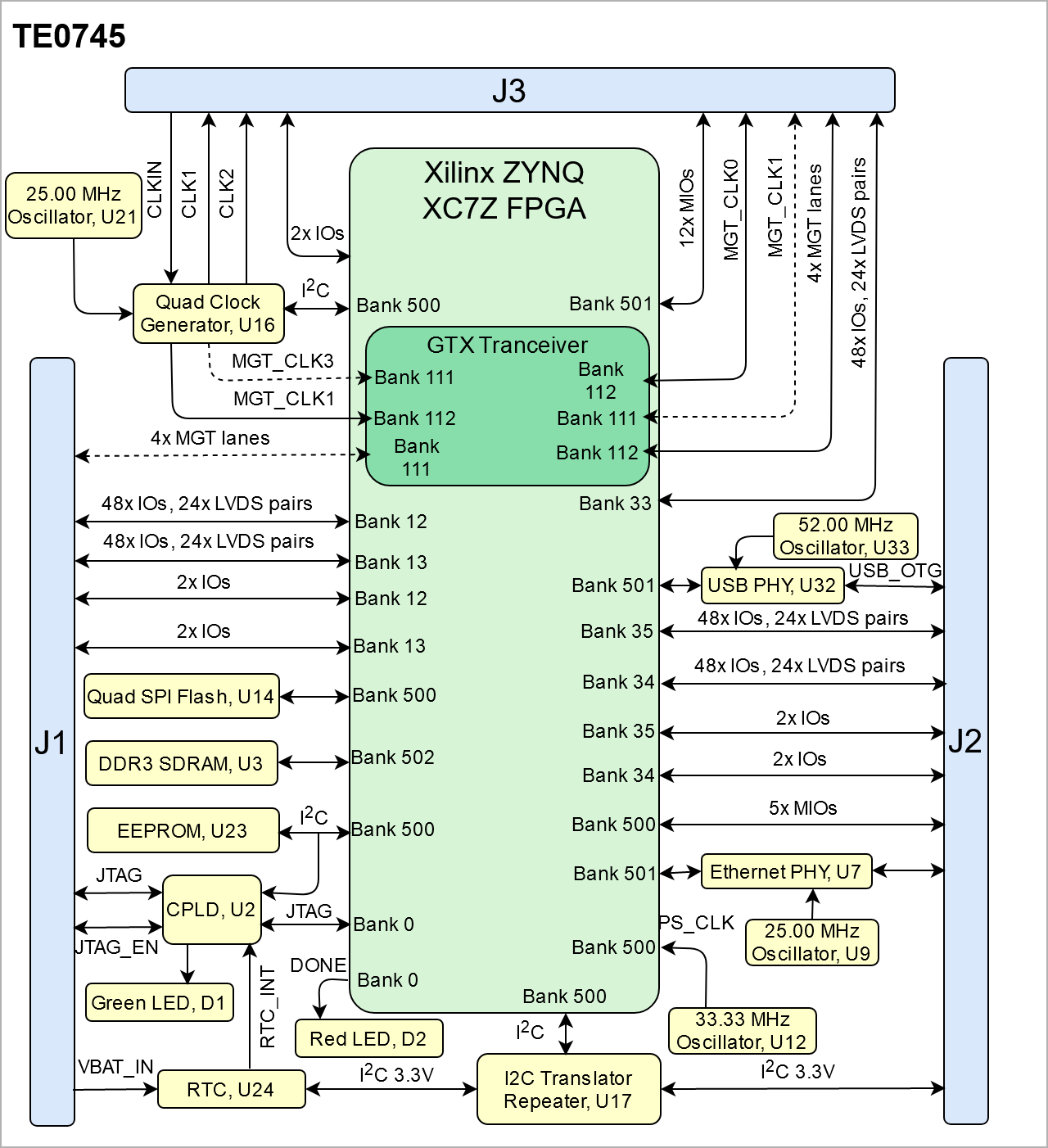
On-board QSPI flash memory (U14) on the TE0745-02 is provided by Micron Serial NOR Flash Memory 256/512 Mbit (32/64 MByte) storage capacity. This non volatile memory is used to store initial FPGA configuration. Besides FPGA configuration, remaining free flash memory can be used for user application and data storage. All four SPI data lines are connected to the FPGA allowing x1, x2 or x4 data bus widths. Maximum data rate depends on the selected bus width and clock frequency used. Quad SPI Flash (U14) is connected to the Zynq PS QSPI0 interface via PS MIO bank 500, pins MIO1 ... MIO6.
| Scroll Title |
|---|
| anchor | Table_OBP_SPI |
|---|
| title | Quad SPI interface MIOs and pins |
|---|
|
| Scroll Table Layout |
|---|
| orientation | portrait |
|---|
| sortDirection | ASC |
|---|
| repeatTableHeaders | default |
|---|
| style | |
|---|
| widths | |
|---|
| sortByColumn | 1 |
|---|
| sortEnabled | false |
|---|
| cellHighlighting | true |
|---|
|
| MIO Pin | Schematic | Notes |
|---|
| MIO1 | SPI-CS |
| | MIO2 | SPI-DQ0/M0 |
| | MIO3 | SPI-DQ1/M1 |
| | MIO4 | SPI-DQ2/M2 |
| | MIO5 | SPI-DQ3/M3 |
| | MIO6 | SPI-SCK/M4 |
|
|
DDR3 SDRAM
The TE0745 SoM has two volatile Intelligent Memory 512 MByte DDR3L-1600 SDRAM IC for storing user application code and data.
- Part number: IM4G16D3FABG-125I
- Supply voltage: 1.5V
- Organization: 256M x 16 bits
DDR3 SDRAM can be varied on demand for other assembly options. DDR3 can have density of maximum 512MB due to available addressing. The maximum possible speed for DDR3 SDRAM is 1600 Mb/s.
RTC
An temperature compensated is used as Real Time Clock (U24). Battery voltage must be supplied to the clock from the base board via pin 'VBAT_IN' (J1-146). Battery backed registers can be accessed over I2C bus at slave address mentioned in the table below. General purpose RAM of the RTC can be accessed at I2C slave address 0x57. RTC IC is supported by Linux so it can be used as hwclock device.
The interrupt line 'RTC_INT' of the RTC is connected to System Controller CPLD bank 3 pin 4.
| Scroll Title |
|---|
| anchor | Table_OBP_I2C_RTC |
|---|
| title | I2C Address for RTC |
|---|
|
| Scroll Table Layout |
|---|
| orientation | portrait |
|---|
| sortDirection | ASC |
|---|
| repeatTableHeaders | default |
|---|
| style | |
|---|
| widths | |
|---|
| sortByColumn | 1 |
|---|
| sortEnabled | false |
|---|
| cellHighlighting | true |
|---|
|
| Schematic | B2B | I2C Address | Designator | Notes |
|---|
I2C_33_SCL | J2-119 | 0x6F | U24 |
| I2C_33_SDA | J2-121 |
|
Programmable PLL Clock
There is a Silicon Labs I2C programmable quad PLL clock generator (U16) on-board. It's output frequencies can be programmed by using the I2C-bus with address 0x70.
A 25.00 MHz (U21) oscillator is connected to pin 3 (IN3) and is used to generate the output clocks.
Once running, the frequency and other parameters can be changed by programming the device using the I2C-bus connected between the Zynq module (master) and reference clock signal generator (slave).
| Scroll Title |
|---|
| anchor | Table_OBP_PLL_CLK |
|---|
| title | Programmable quad PLL clock generator inputs and outputs. |
|---|
|
| Scroll Table Layout |
|---|
| orientation | portrait |
|---|
| sortDirection | ASC |
|---|
| repeatTableHeaders | default |
|---|
| style | |
|---|
| widths | |
|---|
| sortByColumn | 1 |
|---|
| sortEnabled | false |
|---|
| cellHighlighting | true |
|---|
|
U16 Pin
| Signal Name / Description
| Connected To | Direction | Default | Note |
|---|
IN1 | CLKIN_P | B2B, J3-76 | Input |
| Reference input clock from base board. | | IN2 | CLKIN_N | B2B, J3-74 | Input |
| IN3 | Reference input clock. | Oscillator U21, pin 3 | Input |
| 25.000000 MHz oscillator, Si8008BI. | IN4 | - | GND | Input |
| I2C slave device address LSB (0x70 default address). | IN5 | - | Not connected. | Input |
| Not used. | | IN6 | - | GND | Input |
| Not used. | CLK0A | MGT_CLK1_P | Zynq Soc U1, pin U6 | Output | Not programmed | MGT bank 112 reference clock. | | CLK0B | MGT_CLK1_N | Zynq Soc U1, pin U5 | Output | Not programmed | | CLK1A | CLK1_P | B2B, J3-80 | Output | Not programmed | Reference clock output to base board. | | CLK1B | CLK1_N | B2B, J3-82 | Output | Not programmed | | CLK2A | CLK2_P | B2B, J3-86 | Output | Not programmed | Reference clock output to base board. | | CLK2B | CLK2_P | B2B, J3-88 | Output | Not programmed | | CLK3A | MGT_CLK3_P | Zynq Soc U1, pin AA6 | Output | Not programmed | MGT bank 111 reference clock. | | CLK3B | MGT_CLK3_N | Zynq Soc U1, pin AA6 | Output | Not programmed |
|
System Controller CPLD
The System Controller CPLD (U2) is central system management unit where essential control signals are logically linked by the implemented logic in CPLD firmware, which generates output signals to control the system, the on-board peripherals and the interfaces. Interfaces like JTAG and I2C between the on-board peripherals and to the FPGA-module are by-passed, forwarded and controlled by the System Controller CPLD.
Other tasks of the System Controller CPLD are the monitoring of the power-on sequence and to display the programming state of the FPGA module.
For current CPLD Firmware description, check TE0745 CPLD
USB ULPI PHY
Hi-speed USB ULPI PHY (U32) is provided on the board. The ULPI interface is connected to the Zynq PS USB0 via MIO28..39, bank 501 (see also section). The I/O voltage is fixed at 1.8V and PHY reference clock input is supplied from the on-board 52.00 MHz oscillator (U33).
MAC Address EEPROM
A serial EEPROM (U23) contains a globally unique 48-bit node address, which is compatible with EUI-48(TM) specification. The device is organized as two blocks of 128 x 8-bit memory. One of the blocks stores the 48-bit node address and is write protected, the other block is available for application use.
EEPROM
| Scroll Title |
|---|
| anchor | Table_OBP_I2C_EEPROM |
|---|
| title | I2C address for EEPROM |
|---|
|
| Scroll Table Layout |
|---|
| orientation | portrait |
|---|
| sortDirection | ASC |
|---|
| repeatTableHeaders | default |
|---|
| style | |
|---|
| widths | |
|---|
| sortByColumn | 1 |
|---|
| sortEnabled | false |
|---|
| cellHighlighting | true |
|---|
|
| Schematic | MIO | I2C Address | Designator | Notes |
|---|
I2C_SCL | MIO10 | 0x53 | U23 |
| I2C_SDA | MIO11 |
|
Ethernet PHY
On-board Gigabit Ethernet PHY (U7) is provided on the board. The Ethernet PHY RGMII interface is connected to the Zynq Ethernet0 PS GEM0. I/O voltage is fixed at 1.8V for HSTL signaling. The reference clock input of the PHY is supplied from an on-board 25.00 MHz oscillator (U9), the 125MHz output clock signal CLK_125MHZ is connected to the pin J2-150 of B2B connector J2.
| Scroll Title |
|---|
| anchor | Table_SIP_B2B_Eth |
|---|
| title | Ethernet PHY B2B connectors. |
|---|
|
| Scroll Table Layout |
|---|
| orientation | portrait |
|---|
| sortDirection | ASC |
|---|
| repeatTableHeaders | default |
|---|
| style | |
|---|
| widths | |
|---|
| sortByColumn | 1 |
|---|
| sortEnabled | false |
|---|
| cellHighlighting | true |
|---|
|
| Schematic | B2B | Notes |
|---|
| PHY_MDIO | - | Connected to MIO52 | | PHY_MDIO0+/ MDIO0- | J2-120/122 |
| | PHY_MDIO1+/ MDIO1- | J2-126/128 |
| | PHY_MDIO2+/ MDIO2- | J2-132/134 |
| | PHY_MDIO3+/ MDIO3- | J2-138/140 |
| | PHY_LED1 | J2-144 |
| | PHY_LED2 | J2-146 |
| | PHY_LED3 | J2-148 |
| | PHY_CLK125M | J2-150 |
| | PHY_MDC | - | Connected to MIO53 |
|
LEDs
| Scroll Title |
|---|
| anchor | Table_OBP_LED |
|---|
| title | On-board LEDs |
|---|
|
| Scroll Table Layout |
|---|
| orientation | portrait |
|---|
| sortDirection | ASC |
|---|
| repeatTableHeaders | default |
|---|
| style | |
|---|
| widths | |
|---|
| sortByColumn | 1 |
|---|
| sortEnabled | false |
|---|
| cellHighlighting | true |
|---|
|
| Schematic | Color | Connected to | Active level | Note | Note |
|---|
D1 | Green | System Controller CPLD (bank 3, pin 5) | High | System main status LED, blinking indicates system activity |
| D2 | Red | Zynq chip, bank 0 (config bank), 'DONE' pin | Low | Reflects inverted DONE signal. ON when FPGA is not configured, OFF as soon as PL is configured. This LED remains OFF if System Controller CPLD can not power up the PL supply voltage. |
|
|
Clock Sources
| Scroll Title |
|---|
| anchor | Table_OBP_CLK |
|---|
| title | Osillators |
|---|
|
| Scroll Table Layout |
|---|
| orientation | portrait |
|---|
| sortDirection | ASC |
|---|
| repeatTableHeaders | default |
|---|
| style | |
|---|
| widths | |
|---|
| sortByColumn | 1 |
|---|
| sortEnabled | false |
|---|
| cellHighlighting | true |
|---|
|
| Designator | Schematic Name | Frequency | Note |
|---|
| U21 | - | 25.00 MHz | Quad PLL clock generator U16, pin 3 | U12 | PS_CLK | 33.33 MHz | Bank 500 (MIO0 bank), pin B24 | | U33 | OTG-RCLK | 52.00 MHz | USB 2.0 transceiver PHY U32, pin 26 | | U9 | ETH_CLKIN | 25.00 MHz | Gigabit Ethernet PHY U7, pin 34 |
|
Power and Power-On Sequence
Power Supply
Power supply with minimum current capability of 3.0 A for system startup is recommended.
Power Consumption
The maximum power consumption of a module mainly depends on the design which is running on the FPGA.
| Scroll Title |
|---|
| anchor | Table_PWR_PC |
|---|
| title | Power Consumption |
|---|
|
| Scroll Table Layout |
|---|
| orientation | portrait |
|---|
| sortDirection | ASC |
|---|
| repeatTableHeaders | default |
|---|
| style | |
|---|
| widths | |
|---|
| sortByColumn | 1 |
|---|
| sortEnabled | false |
|---|
| cellHighlighting | true |
|---|
|
| Power Input Pin | Typical Current |
|---|
| PL_VIN | TBD* | | PS_VIN | TBD* | | PS_3.3V | TBD* |
|
* TBD - To Be Determined
For the lowest power consumption and highest efficiency of on board DC-DC regulators it is recommended to powering the module from one single 3.3V supply. All input power supplies have a nominal value of 3.3V. Although the input power supplies can be powered up in any order, it is recommended to power them up simultaneously.
The on-board voltages of the TE0745 SoC module will be powered-up in order of a determined sequence after the external voltages 'PL_VIN', 'PS_VIN' and 'PS_3.3V' are available. All those power-rails can be powered up, with 3.3V power sources, also shared.
| Warning |
|---|
| To avoid any damage to the module, check for stabilized on-board voltages should be carried out(i.e. power good and enable signals) before powering up any SoC's I/O bank voltages VCCO_x. All I/Os should be tri-stated during power-on sequence. |
Core voltages and main supply voltages have to reach stable state and their "Power Good"-signals have to be asserted before other voltages like PL bank's I/O voltages can be powered up.
It is important that all baseboard I/Os are tri-stated at power-on until the "Power Good"-signals 'PWR_PS_OK' (J2-139) and 'PWR_PL_OK' (J2-135) are high, meaning that all on-module voltages have become stable and module is properly powered up.
Power Distribution Dependencies
| Scroll Title |
|---|
| anchor | Figure_PWR_PD |
|---|
| title | Power Distribution |
|---|
|
| Scroll Ignore |
|---|
| scroll-pdf | true |
|---|
| scroll-office | true |
|---|
| scroll-chm | true |
|---|
| scroll-docbook | true |
|---|
| scroll-eclipsehelp | true |
|---|
| scroll-epub | true |
|---|
| scroll-html | true |
|---|
| | draw.io Diagram |
|---|
| border | false |
|---|
| viewerToolbar | true |
|---|
| |
|---|
| fitWindow | false |
|---|
| diagramDisplayName | |
|---|
| lbox | true |
|---|
| revision | 1 |
|---|
| diagramName | TE0745_PWR_PD |
|---|
| simpleViewer | false |
|---|
| width | |
|---|
| links | auto |
|---|
| tbstyle | hidden |
|---|
| diagramWidth | 641 |
|---|
|
|
| Scroll Only |
|---|
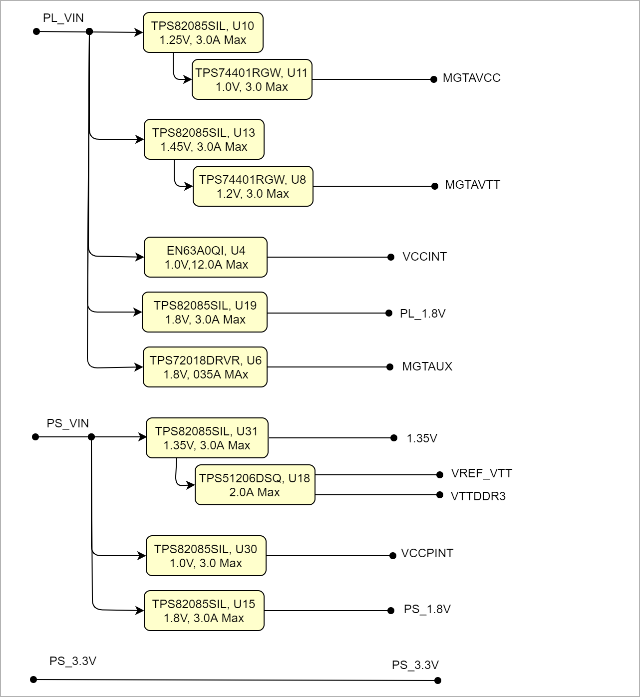 Image Modified Image Modified
|
|
| Note |
|---|
Current rating of Samtec Razor Beam LP Terminal/Socket Strip ST5/SS5 B2B connectors is 1.5 A per pin (1 pin powered per row). |
Power-On Sequence
The TE0745 SoM meets the recommended criteria to power up the Xilinx Zynq MPSoC properly by keeping a specific sequence of enabling the on-board DCDC converters dedicated to the particular functional units of the Zynq chip and powering up the on-board voltages.
Following diagram clarifies the sequence of enabling the particular on-board voltages, which will power-up in descending order as listed in the blocks of the diagram:
| Scroll Title |
|---|
| anchor | Figure_PWR_PS |
|---|
| title | Power Sequency |
|---|
|
| Scroll Ignore |
|---|
| draw.io Diagram |
|---|
| border | false |
|---|
| viewerToolbar | true |
|---|
| |
|---|
| fitWindow | false |
|---|
| diagramDisplayName | |
|---|
| lbox | true |
|---|
| revision | 1 |
|---|
| diagramName | TE0745_PWR_PS |
|---|
| simpleViewer | false |
|---|
| width | |
|---|
| links | auto |
|---|
| tbstyle | hidden |
|---|
| diagramWidth | 640 |
|---|
|
|
| Scroll Only |
|---|
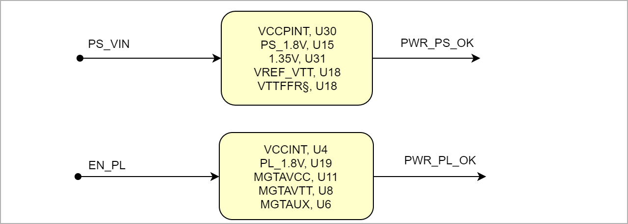 Image Modified Image Modified
|
|
The Enable-Signal 'EN_PL' is permanently logic high in standard SC-CPLD firmware. The "Power Good"-signals 'PWR_PS_OK' and 'PWR_PL_OK' (latter low-active, extern pull-up needed) are available B2B-connector J2 (pins J2-139, J2-135) and on the SC-CPLD.
Voltage Monitor Circuit
The voltages 'VCCPINT' and 'PS_1.8V' are monitored by the voltage monitor circuit U41, which generates the POR_B reset signal at Power-On. A manual reset is also possible by driving the MR-pin (available on J2-131 or SC-CPLD) to GND. Leave this pin unconnected or connect to VDD (PS_1.8V) when unused.
| Scroll Title |
|---|
| anchor | Figure_PWR_VMC |
|---|
| title | Voltage Monitor Circuit |
|---|
|
| Scroll Ignore |
|---|
| draw.io Diagram |
|---|
| border | false |
|---|
| viewerToolbar | true |
|---|
| |
|---|
| fitWindow | false |
|---|
| diagramDisplayName | |
|---|
| lbox | true |
|---|
| revision | 1 |
|---|
| diagramName | TE0745_PWR_PM |
|---|
| simpleViewer | false |
|---|
| width | |
|---|
| links | auto |
|---|
| tbstyle | hidden |
|---|
| diagramWidth | 641 |
|---|
|
|
| Scroll Only |
|---|
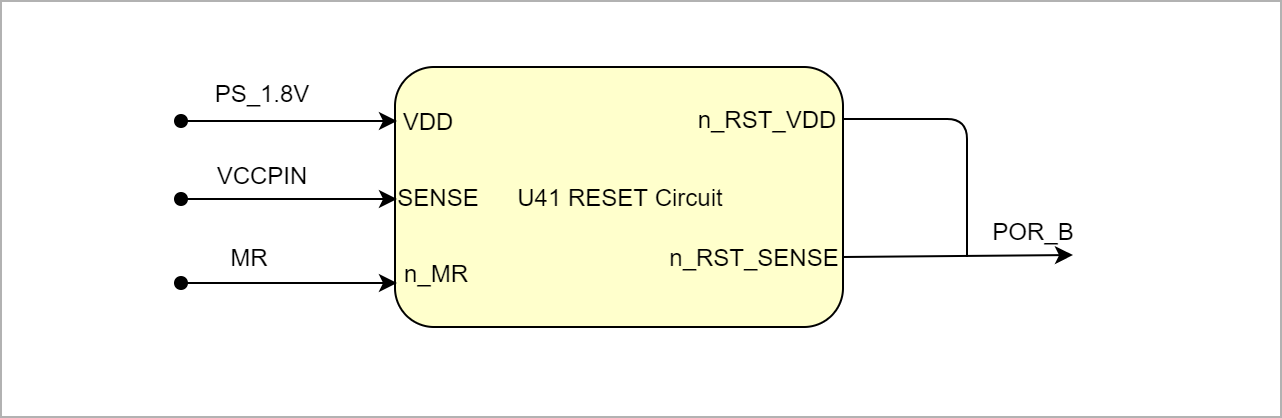 Image Modified Image Modified
|
|
Power Rails
| Scroll Title |
|---|
| anchor | Table_PWR_PR |
|---|
| title | Module power rails. |
|---|
|
| Scroll Table Layout |
|---|
| orientation | portrait |
|---|
| sortDirection | ASC |
|---|
| repeatTableHeaders | default |
|---|
| style | |
|---|
| widths | |
|---|
| sortByColumn | 1 |
|---|
| sortEnabled | false |
|---|
| cellHighlighting | true |
|---|
|
| Power Rail Name | B2B Connector JM1 Pin | B2B Connector JM2 Pin | B2B Connector JM3 Pin | Direction | Notes |
|---|
| PL_VIN | 147, 149, 151, 153,
155, 157, 159 | - | - | Input | module supply voltage | | PS_VIN | - | 154, 156, 158 | - | Input | module supply voltage | | PS_3.3V | - | 160 | - | Input | module supply voltage | | VCCIO12 | 54, 55 | - | - | Input | high range bank I/O voltage | | VCCIO13 | 112, 113 | - | - | Input | high range bank I/O voltage | | VCCIO33 | - | - | 115, 120 | Input | high performance bank I/O voltage | | VCCIO34 | - | 29, 30 | - | Input | high performance bank I/O voltage | | VCCIO35 | - | 87, 88 | - | Input | high performance bank I/O voltage | | VBAT_IN | 146 | - | - | Input | RTC (battery-backed) supply voltage | | PS_1.8V | - | 130 | - | Output | internal 1.8V voltage level (Process System) | | PL_1.8V | - | - | 84,85 | Output | internal 1.8V voltage level (FPGA) |
|
Bank Voltages
| Scroll Title |
|---|
| anchor | Table_PWR_BV |
|---|
| title | Zynq SoC bank voltages. |
|---|
|
| Scroll Table Layout |
|---|
| orientation | portrait |
|---|
| sortDirection | ASC |
|---|
| repeatTableHeaders | default |
|---|
| style | |
|---|
| widths | |
|---|
| sortByColumn | 1 |
|---|
| sortEnabled | false |
|---|
| cellHighlighting | true |
|---|
|
| Schematic Name | | Notes |
|---|
| 0 (config) | VCCIO_0 | PL_1.8V, if R67 is equipped
PS_1.8V, if R68 is equipped | - | | 500 (MIO0) | PS_1.8V | 1.8V | - | | 501 (MIO1) | PS_1.8V | 1.8V | - | | 502 (DDR3) | 1.35V | 1.35V | - | | 12 HR | VCCIO_12 | User | HR: 1.2V to 3.3V | | 13 HR | VCCIO_13 | User | HR: 1.2V to 3.3V
| | 33 HP | VCCIO_33 | User | HP: 1.2V to 1.8V |
|
Board to Board Connectors
| Page properties |
|---|
|
- This section is optional and only for modules.
use "include page" macro and link to the general B2B connector page of the module series, For example: 6 x 6 SoM LSHM B2B Connectors
| Include Page |
|---|
| 6 x 6 SoM LSHM B2B Connectors |
|---|
| 6 x 6 SoM LSHM B2B Connectors |
|---|
|
|
| Include Page |
|---|
| 5.2 x 7.6 SoM ST5 and SS5 B2B Connectors |
|---|
| 5.2 x 7.6 SoM ST5 and SS5 B2B Connectors |
|---|
|
Technical Specifications
Absolute Maximum Ratings
| Scroll Title |
|---|
| anchor | Table_TS_AMR |
|---|
| title | PS absolute maximum ratings |
|---|
|
| Scroll Table Layout |
|---|
| orientation | portrait |
|---|
| sortDirection | ASC |
|---|
| repeatTableHeaders | default |
|---|
| style | |
|---|
| widths | |
|---|
| sortByColumn | 1 |
|---|
| sortEnabled | false |
|---|
| cellHighlighting | true |
|---|
|
| Symbols | Description | Min | Max | Unit |
|---|
| PL_VIN | -0.3 | 5 | V | TI TPS720 data sheet | | PS_VIN | -0.3 | 7 | V | TI TPS82085 data sheet | | PS_3.3V | 3.135 | 3.465 | V | 3.3V nominal ± 5%
| | VBAT supply voltage | -1 | 6.0 | V | ISL12020MIRZ data sheet | | PL IO bank supply voltage for HR I/O banks (VCCO) | -0.5 | 3.6 | V | - | PL IO bank supply voltage for HP I/O banks (VCCO) | -0.5 | 2.0 | V | - | | I/O input voltage for HR I/O banks | -0.4 | VCCO_X+0.55 | V | - | | I/O input voltage for HP I/O banks | -0.55 | VCCO_X+0.55 | V | - | | GT receiver (RXP/RXN) and transmitter (TXP/TXN) | -0.5 | 1.26 | V | - | Voltage on module JTAG pins | -0.3 | 3.6 | V | MachX02 Family data sheet | Storage temperature | -40 | +128 | °C | Limits of ISL12020MIRZ RTC chip. | | Storage temperature without the ISL12020MIRZ | -55 | +100 | °C | Limits of DDR3 memory chip. |
|
Attention: PS_3.3V is directly connected to numerous on-board peripherals as supply and I/O voltage.
Recommended Operating Conditions
Operating temperature range depends also on customer design and cooling solution. Please contact us for options.
| Scroll Title |
|---|
| anchor | Table_TS_ROC |
|---|
| title | Recommended operating conditions. |
|---|
|
| Scroll Table Layout |
|---|
| orientation | portrait |
|---|
| sortDirection | ASC |
|---|
| repeatTableHeaders | default |
|---|
| style | |
|---|
| widths | |
|---|
| sortByColumn | 1 |
|---|
| sortEnabled | false |
|---|
| cellHighlighting | true |
|---|
|
| Parameter | Min | Max | Units | Reference Document |
|
|---|
| PL_VIN | 3. |
|