Page History
...
| CPLD functionality | interface | designated CPLD pins | connected with | Note |
|---|---|---|---|---|
Table 11: System Controller CPLD functionalities
Clocking
The TEC0330 FPGA board has a sophisticated clock generation and conditioning system to meet the requirements of the Xilinx Virtex-7 GTH units with data transmission rates up to 13.1 Gb/s.
Clock sources
...
PS CLK
...
33.3333 MHz
...
U11
...
PS_CLK
...
PS subsystem main clock.
...
ETH PHY reference
...
25 MHz
...
U9
...
-
...
USB PHY reference
...
52 MHz
...
U15
...
-
...
PLL reference
...
25 MHz
...
U18
...
-
...
GT REFCLK0
...
-
...
B2B
...
U9/V9
...
Externally supplied from baseboard.
...
GT REFCLK1
...
125 MHz
...
U10 Si5338
...
U5/V5
...
Default clock is 125 MHz.
PLL - Phase-Locked Loop
There is a Silicon Labs I2C programmable clock generator Si5338A (U10) chip on the module. It's output frequencies can be programmed using the I2C bus address 0x70.
PLL connection
...
IN1/IN2
...
Externally supplied
...
Needs decoupling on base board.
...
IN3
...
25MHz
...
Fixed input clock.
...
IN4
...
-
...
-
...
IN5/IN6
...
125MHz
...
Ethernet PHY output clock.
...
CLK0
...
-
...
Not used, disabled.
...
CLK1
...
-
...
Not used, disabled.
...
CLK2 A/B
...
125MHz
...
MGT reference clock 1.
...
CLK3A
...
-
...
Bank 34 clock input, default disabled, User clock.
...
CLK3B
...
-
...
Not used, disabled.
Power and Power-On Sequence
...
Table 11: System Controller CPLD functionalities
Clocking
Clock sources
The SoC module has the following sources to be provided with extern reference clock signals and on-board clock oscillators:
| Clock source | Schematic name | Frequency | Clock input destination | Note |
|---|---|---|---|---|
| B2B connector J3, pin J3-74/J3-76 | CLKIN_N, CLKIN_P | user | Quad PLL clock Generator U16, pin 1/2 | - |
| B2B connector J3, pin J3-75/J3-77 | MGT_CLK0_P, MGT_CLK0_N | user | MGT-bank 112, pin R6/R5 | - |
| B2B connector J3, pin J3-81/J3-83 | MGT_CLK2_P, MGT_CLK2_N | user | MGT-bank 111, pin W6/W5 | - |
| SiTime SiT8008BI oscillator, U21 | - | 25.000 MHz | Quad PLL clock Generator U16, pin 3 | - |
SiTime SiT8008BI oscillator, U12 | PS_CLK | 33.333 MHz | Bank 500 (MIO0 bank), pin B24 | - |
| SiTime SiT8008BI oscillator, U23 | OTG-RCLK | 52.000 MHz | USB 2.0 Transceiver PHY U32, pin 26 | - |
| SiTime SiT8008BI oscillator, U9 | ETH_CLKIN | 25.000 MHz | Gbit Ethernet PHY U7, pin 34 | - |
Table 12: Clock sources overview
Programmable PLL Clock (Phase-Locked Loop)
There is a Silicon Labs I²C programmable quad PLL clock generator Si5338A (U16) on-board. It's output frequencies can be programmed by using the I²C-bus with address 0x70.
A 25 MHz (U21) oscillator is connected to pin 3 (IN3) and is used to generate the output clocks.
Once running, the frequency and other parameters can be changed by programming the device using the I²C-bus connected between the Zynq-module (master) and reference clock signal generator (slave).
| Si5338A (U13) input | signal schematic name | Note |
|---|---|---|
IN1/IN2 | CLKIN_P, CLKIN_N | reference clock signal from B2B connector J3, pin J3-74/J3-76 (base board decoupling capacitors and termination resistor necessary) |
IN3 | reference clock signal from oscillator SiTime SiT8008BI (U21) | 25.000 MHz fixed frequency |
IN4/IN6 | pins put to GND | LSB (pin 'IN4') of the default I²C-adress 0x70 is zero |
IN5 | not connected | - |
| Si5338A (U13) output | signal schematic name | Note |
CLK0 A/B | MGTCLK1_P, MGTCLK1_N | reference clock signal to MGT-bank 112, pin U6/U5 (100 nF decoupling capacitors) |
CLK1 A/B | CLK1_P, CLK1_N | clock signal routed to B2B connector, pin J3-80/J3-82 |
CLK2 A/B | CLK2_P, CLK2_N | clock signal routed to B2B connector, pin J3-86/J3-88 |
| CLK3 A/B | MGTCLK3_P, MGTCLK3_N | reference clock signal to MGT-bank 111, pin AA6/AA5 (100 nF decoupling capacitors) |
Table 13: Pin description of PLL clock generator Si5338A
Power and Power-On Sequence
...
Power Supply
Power supply with minimum current capability of 3A for system startup is recommended.
...
| Parameter | Min | Max | Units | Notes | Reference Document |
|---|---|---|---|---|---|
| VIN supply voltage | 2.5 | 5.5 | V | ||
| 3.3VIN supply voltage | 3.135 | 3.465 | V | ||
| VBAT_IN supply voltage | 2.7 | 5.5 | V | ||
PL I/O bank supply voltage for HR I/O banks (VCCO) | 1.14 | 3.465 | V | Xilinx datasheet DS191 | |
PL I/O bank supply voltage for HP I/O banks (VCCO) | 1.14 | 1.89 | V | TE0715-xx-15 does not have HP banks | Xilinx datasheet DS191 |
| I/O input voltage for HR I/O banks | (*) | (*) | V | (*) Check datasheet | Xilinx datasheet DS191 or DS187 |
| I/O input voltage for HP I/O banks | (*) | (*) | V | TE0715-xx-15 does not have HP banks (*) Check datasheet | Xilinx datasheet DS191 |
| Voltage on Module JTAG pins | 3.135 | 3.465 | V | VCCO_0 is 3.3 V nominal |
Absolute Maximum Ratings
...
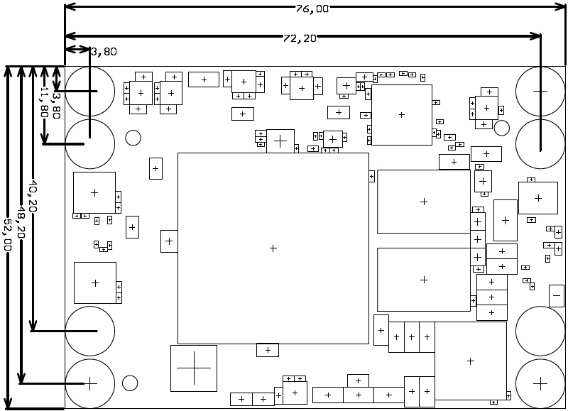
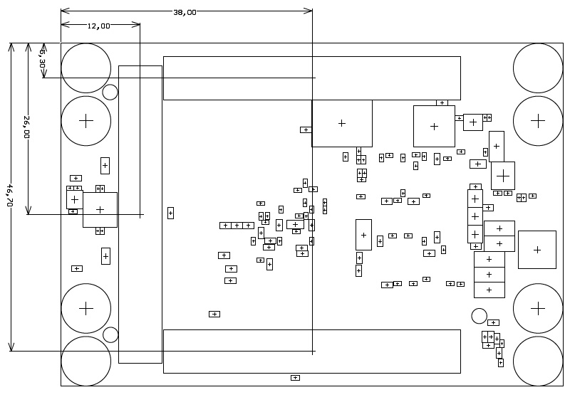
Physical Dimensions
Module size: 52 mm × 76 mm. Please download the assembly diagram for exact numbers
Mating height with standard connectors: 4mm
PCB thickness: 1.6mm
Highest part on PCB: approx. 3mm. Please download the step model for exact numbers
All dimensions are given in millimeters.
Operating Temperature Ranges
...
The module operating temperature range depends also on customer design and cooling solution. Please contact us for options.
Weight
.. 24 g - Plain module.. g - Set of bolts and nuts
Revision History
Hardware Revision History
...
| Date | Revision | Contributors | Description |
|---|---|---|---|
| 2017-03-28 | Ali Naseri, Jan Kumann | first TRM release | |
| 2017-02-05 | V1
| Jan Kumann | Initial document. |
...
Overview
Content Tools