Page History
...
The I/O signals are routed from the SoC's PL banks as LVDS-pairs to the B2B connector.
| Bank | Type | B2B Connector | I/O signal count | LVDS-pairs count | VCCO bank voltage | Notes |
|---|---|---|---|---|---|---|
| 12 | HR | J1 | 50 | 24 | user (VCCIO_12) | supported voltages from 1.2V to 3.3V |
| 13 | HR | J1 | 50 | 24 | user (VCCIO_13) | supported voltages from 1.2V to 3.3V |
| 34 |
| HP | J2 | 50 | 24 | user (VCCIO_34) | supported voltages from 1.2V to |
| 1. |
| 8V |
| 35 |
| HP | J2 | 50 | 24 | user (VCCIO_35) | supported voltages from 1.2V to |
| 1. |
| 8V | ||||||
| 500 | MIO | J2 | 5 | - | 1.8V | - |
| 501 | MIO | J3 | 12 | - | 1.8V | - |
Table 2: B2B connector pin-outs of available PL and PS banks of the SoC module
...
The B2B connector provides further interfaces like 'JTAG' and 'I²C' to the System Controller CPLD:
| Interfaces | I/O signal count | pin schematic names / B2B pins | connected with | Notes | ||
|---|---|---|---|---|---|---|
| JTAG | 5 | TMS, pin J1-144 TDI, pin J1-142 TDO, pin J1-145 TCK, pin J1-143 JTAG_EN, pin J1-148 | SC CPLD, bank 0 |
At normal operation the JTAG-signals will be forwarded to the SoC module. Else the JTAG_EN pin must be high or open to update the CPLD firmware via JTAG-interface. VCCIO: PS_3.3V | ||
| I²C | 2 | I2C_33_SCL, pin J2-119 I2C_33_SDA, pin J2-121 | RTC, U24 SC CPLD, U2 MAC Address EEPROM, U23 Zynq-module, U1 Quad programmable PLL clock generator, U16 | The I²C-interface of the RTC U24 (pin 12: SCL, pin 11: SDA) and the B2B-connector J2 are operating with the reference voltage PS_3.3V. Following component's I²C-interfaces are operating with the reference voltage PS_1.8V (voltage level shifting 3.3V ↔ 1.8V via I²C bus repeater U17):
Component's I²C Addresses:
| ||
| control lines | 5 | RST_IN_N, pin J2-131 | SC CPLD bank 0, pins 25; Reset Circuit U41, pin 3 | Low-active Power-On reset pin, controls POR_B-signal (bank 500, pin C23) of Zynq-chip. | ||
| PS_SRST, pin J2-152 | SC CPLD bank 2, pin 12; Zynq-chip bank 501, pin A22 | Low-active system-reset pin of Zynq-chip. | ||||
| BOOTMODE, pin J2-133 | Zynq-chip bank 500, pin F24 | Control line which sets in conjunction with signal 'BOOTMODE1' the boot source of the Zynq-chip. See section "Boot Modes". | ||||
| PWR_PL_OK, pin J2-135 | SC CPLD bank 0, pin 27; PG-signal DCDC-converter U8, pin 9 | Indicates stable state of PL supply voltage (low-active) after power-up sequence. | ||||
| PWR_PS_OK, pin J2-139 | SC CPLD bank 0, pin 28; PG-signal DCDC-converter U31, pin 2 | Indicates stable state of PS supply voltage (low-active) after power-up sequence. |
Table 4: B2B connector pin-outs of available interfaces
...
| PHY Pin | ZYNQ Pin | B2B Name | Notes |
|---|---|---|---|
| ULPI | MIO28..39 | - | Zynq USB0 MIO pins are connected to the PHY |
| REFCLK | - | - | 52MHz from on board oscillator (U33) |
| REFSEL[0..2] | - | - | all pins set to GND selects the external reference clock frequency @52MHz |
| RESETB | MIO7 | - | low-active reset line |
| CLKOUT | MIO36 | - | set to VDDIO high (1.8V level (VDDIO)) to select reference clock operation mode |
| DP, DM | - | OTG_D_P, OTG_D_N, pin J2-149 / J2-151 | USB data lines |
| CPEN | - | VBUS_V_EN, pin J2-141 | External USB power switch active high enable signal |
| VBUS | - | USB_VBUS, pin J2-145 | Connect to USB VBUS via a series of resistors, see reference schematics |
| ID | - | OTG_ID, pin J2-143 | For an A-Device connect to ground, for a B-Device left floating |
...
Lowest power consumption and highest efficiency of on board DC/DC regulators it is recommended to powering the module from one single 3.3V supply. All input power supplies have a nominal value of 3.3V. Although the input power supplies can be powered up in any order, it is recommended to power them up simultaneously.
Power-On Sequence
It is important that all baseboard I/Os are 3-stated at power-on until System Controller sets PGOOD signal high (B2B connector JM1, pin 30), or 3.3V is present on B2B connector JM2 pins 10 and 12, meaning that all on-module voltages have become stable and module is properly powered up.
See Xilinx datasheet DS191 (for XC7Z030) for additional information. User should also check related base board documentation when intending base board design for TE0745 module.
The on-board voltages of the TEC0330 FPGA board The on-board voltages of the TE0745 SoC module will be powered-up in order of a determined sequence after the external voltages '12V' on connector J5 and '3V3PCI' on connector J1 'PL_VIN', 'PS_VIN' and 'PS_3.3V' are available.
| Warning |
|---|
| To avoid any demages to the SoM, check for stabilized on-board voltages in steady state before powering up the SoC's I/O bank voltages VCCO_x. |
Core voltages and main supply voltages Core voltages and main supply voltages have to reach stable state and their "Power Good"-signals have to be asserted before other voltages like PL bank's I/O voltages can be powered up.
Following diagram clarifies the sequence of enabling the particular on-board voltages:
Power-up sequence at start-up
The Trenz TE0782 SoM is equipped with two quad DC/DC-voltage-regulators to generate the required on-board voltages with the values 1V, 3.3V, 1.8V, 1.2V_MGT, 1V_MGT.
There are also additional voltage regulators on board to generate the voltages 1.5V, VTT, VTTREF and 1.8V_MGT.
On this SoM the sequence of powering up of the required on-board voltages is handled internally by the system controller CPLD processing the "POWER GOOD"-signals from the voltage-regulators.
To avoid any demages to the SoM, check for stabilized on-board voltages in steady state before powering up the SoC's I/O bank voltages VCCIO.
The "POWER GOOD"-signals can be checked on the system controller CPLD.
...
It is important that all baseboard I/Os are 3-stated at power-on until the "Power Good"-signals 'PWR_PS_OK' (J2-139) and 'PWR_PL_OK' (J2-135) are high, meaning that all on-module voltages have become stable and module is properly powered up.
Following diagram clarifies the sequence of enabling the particular on-board voltages:
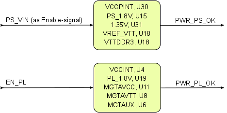
Figure 3: Power-up sequence diagram
See Xilinx datasheet DS191 for additional information. User should also check related base board documentation when intending base board design for TE0745 module.
Power Rails
Voltages on B2B | B2B J1 Pin | B2B J2 Pin | B2B J3 Pin | Input/ | Note |
|---|---|---|---|---|---|
| PL_VIN | 147, 149, 151, 153, | - | - | Input | supply voltage |
| PS_VIN | - | 154, 156, 158 | - | Input | supply voltage |
| PS_3.3V | - | 160 | - | Input | supply voltage |
| VCCIO12 | 54, 55 | - | - | Input | high range bank voltage |
| VCCIO13 | 112, 113 | - | - | Input | high range bank voltage |
| VCCIO33 | - | - | 115, 120 | Input | high performance bank voltage |
| VCCIO34 | 29, 30 | - | Input | high performance bank voltage | |
| VCCIO35 | 87, 88 | - | Input | high performance bank voltage | |
| VBAT_IN | 146 | - | - | Input | RTC battery-buffer supply voltage |
| PS_1.8V | - | 130 | - | Output | internal 1.8V voltage level (Process System supply) |
...
Technical Specification
Absolute Maximum Ratings
Parameter | Min | Max | Units | Notes |
|---|---|---|---|---|
| PL_VIN | ||||
| PS_VIN | ||||
| PS_3.3V | ||||
| VBAT supply voltage | -1 | 6.0 | V | - |
| PL IO bank supply voltage for HR I/O banks (VCCO) | -0.5 | 3.6 | V | - |
PL IO bank supply voltage for HP | -0.5 | 2.0 | V | - |
| I/O input voltage for HR I/O banks | -0.4 | VCCO_X+0.55 | V | - |
| I/O input voltage for HP I/O banks | -0.55 | VCCO_X+0.55 | V | - |
| GT receiver (RXP/RXN) and transmitter (TXP/TXN) | -0.5 | 1.26 | V | - |
Voltage on module JTAG pins | -0.3 | 3.6 | V | MachX02 Family Data Sheet |
Storage temperature | -40 | +85 | °C | - |
| Storage temperature without the ISL12020MIRZ | -55 | +100 | °C | - |
| Note |
|---|
| Assembly variants for higher storage temperature range are available on request. |
Recommended Operating Conditions
| Parameter | Min | Max | Units | Notes | Reference Document |
|---|---|---|---|---|---|
| PL_VIN | |||||
| PS_VIN | |||||
| PS_3.3V | |||||
| VBAT_IN supply voltage | 2.7 | 5.5 | V | - | - |
PL I/O bank supply voltage for HR | 1.14 | 3.465 | V | - | Xilinx datasheet DS191 |
PL I/O bank supply voltage for HP | 1.14 | 1.89 | V | - | Xilinx datasheet DS191 |
| I/O input voltage for HR I/O banks | (*) | (*) | V | (*) Check datasheet | Xilinx datasheet DS191 |
| I/O input voltage for HP I/O banks | (*) | (*) | V | (*) Check datasheet | Xilinx datasheet DS191 |
| GT receiver (RXP/RXN) and transmitter (TXP/TXN) | (*) | (*) | V | (*) Check datasheet | Xilinx datasheet DS191 |
| Voltage on Module JTAG pins | 3.135 | 3.6 | V | JTAG-signals forwarded to Zynq-module config bank 0 | MachX02 Family Data Sheet |
| Note |
|---|
| Please check Xilinx datasheet DS191 (for XC7Z030) for complete list of absolute maximum and recommended operating ratings. |
...
Overview
Content Tools