Page History
...
Industrial-grade Xilinx Zynq-7000 (Z-7030, Z-7035, Z-7045) SoMSoC module
- Rugged for shock and high vibration
- 10/100/1000 Mbps Ethernet transceiver PHY
- EEPROM for storing Ethernet MAC Address
- 16-Bit wide 1GB DDR3 SDRAM
- 32 MByte QSPI flash memory
- Programmable clock generator
- Plug-on module with 3 × 160-pin high-speed hermaphroditic strips
- 132 FPGA I/Os (65 LVDS pairs possible) and 14 PS MIO available on B2B connectors
- 8 GTX (high-performance transceiver) lanes
- USB 2.0 OTG high-speed PHY
- On-board high-efficiency DC-DC converters
- System management
- eFUSE bit-stream encryption
- AES bit-stream encryption
- Temperature compensated RTC (real-time clock)
- User LED
- Evenly-spread supply pins for good signal integrity
...
| Warning |
|---|
| To avoid any demages to the SoMSoC module, check for stabilized on-board voltages in steady state before powering up the SoC's I/O bank voltages VCCO_x. |
...
Voltages on B2B | B2B J1 Pin | B2B J2 Pin | B2B J3 Pin | Input/ | Note |
|---|---|---|---|---|---|
| PL_VIN | 147, 149, 151, 153, | - | - | Input | supply voltage |
| PS_VIN | - | 154, 156, 158 | - | Input | supply voltage |
| PS_3.3V | - | 160 | - | Input | supply voltage |
| VCCIO12 | 54, 55 | - | - | Input | high range bank voltage |
| VCCIO13 | 112, 113 | - | - | Input | high range bank voltage |
| VCCIO33 | - | - | 115, 120 | Input | high performance bank voltage |
| VCCIO34 | 29, 30 | - | Input | high performance bank voltage | |
| VCCIO35 | 87, 88 | - | Input | high performance bank voltage | |
| VBAT_IN | 146 | - | - | Input | RTC (battery-buffer buffered) supply voltage |
| PS_1.8V | - | 130 | - | Output | internal 1.8V voltage level (Process System supply) |
...
Parameter | Min | Max | Units | Notes | |||
|---|---|---|---|---|---|---|---|
| PL_VIN | -0.3 | 5 | V | TPS720 data sheet | |||
| PS_VIN | -0.3 | 7 | V | TPS82085 data sheet | |||
| PS_3.3V | 3.135 | 3.465 | V | 3.3V nominal ± 5% | |||
| VBAT supply voltage | -1 | 6.0 | V | -ISL12020MIRZ data sheet | |||
| PL IO bank supply voltage for HR I/O banks (VCCO) | -0.5 | 3.6 | V | - | |||
PL IO bank supply voltage for HP | -0.5 | 2.0 | V | - | |||
| I/O input voltage for HR I/O banks | -0.4 | VCCO_X+0.55 | V | - | |||
| I/O input voltage for HP I/O banks | -0.55 | VCCO_X+0.55 | V | - | |||
| GT receiver (RXP/RXN) and transmitter (TXP/TXN) | -0.5 | 1.26 | V | - | |||
Voltage on module JTAG pins | -0.3 | 3.6 | V | MachX02 Family data sheet | |||
Storage temperature | -40 | +85 | °C | ISL12020MIRZ data sheet | |||
| Storage temperature without the ISL12020MIRZ | -55 | +100 | °C | Intelligent memory datasheet |
...
| Parameter | Min | Max | Units | Notes | Reference Document | ||||
|---|---|---|---|---|---|---|---|---|---|
| PL_VIN | 3.3 | 4.5 | V | - | TPS720 data sheet | ||||
| PS_VIN | 3.3 | 6.0 | V | - | TPS82085 data sheet | ||||
| PS_3.3V | 3.135 | 3.465 | V | - | 3.3V nominal ± 5% | ||||
| VBAT_IN supply voltage | 2.7 | 5.5 | V | - | -ISL12020MIRZ data sheet | ||||
PL I/O bank supply voltage for HR | 1.14 | 3.465 | V | - | Xilinx datasheet DS191 | ||||
PL I/O bank supply voltage for HP | 1.14 | 1.89 | V | - | Xilinx datasheet DS191 | ||||
| I/O input voltage for HR I/O banks | (*) | -0.20 | VCCO_X+0.20(*) | V | (*) Check datasheet- | Xilinx datasheet DS191 | |||
| I/O input voltage for HP I/O banks | (*) | -0.20 | VCCO_X+0.20(*) | V | (*) Check datasheet- | Xilinx datasheet DS191 | |||
| GT receiver (RXP/RXN) and transmitter (TXP/TXN) | (*) | (*) | V | (*) Check datasheet | Xilinx datasheet DS191 | ||||
| Voltage on Module JTAG pins | 3.135 | 3.6 | V | JTAG-signals forwarded to Zynq-module config bank 0 | MachX02 Family Data Sheet |
...
All dimensions are given in millimeters.
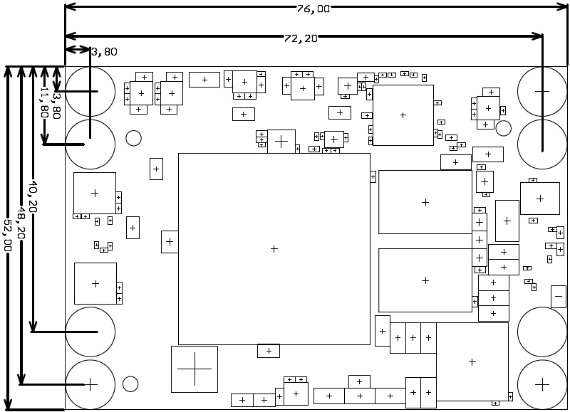
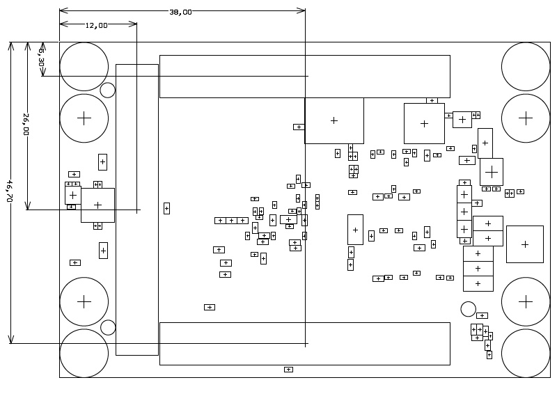
Figure 4: Physical dimensions of the TE0745 SoC module
Operating Temperature Ranges
...
Overview
Content Tools