Page History
...
- Xilinx ZYNQ-7000 family SoC, U1
- 256 Mbit Quad SPI Flash Memory memory Micron N25Q256A, U12
- Reference clock signal oscillator SiTime SiT8008BI @33.333 MHz, U12
- Reference clock signal oscillator SiTime SiT8008BI @25.000 MHz, U9
- Marvell Alaska 88E1512 Gigabit Ethernet PHY, U3
- Intelligent Memory 512 MByte DDR3L-1600 SDRAM (8 Banks a 32 MWords, 16 Bit Word-Widthbit word width), U3
- TI TPS51206 DDR3 Memory Termination Regulator memory termination regulator with buffered reference votlage voltage VTTREF, U18
- Intersil ISL12020MIRZ Real-Time-Clock, U24
- TI TCA9517 Levellevel-shifting I²C I2C bus repeater, U17
- Red LED, D2 red
- Green LED, D1 green
- Intelligent Memory 512 MByte DDR3L-1600 SDRAM (8 Banks banks a 32 MWords, 16 Bit Word-Width), U5
- Altera Enpirion EN63A0QI 12A DCDC DC-DC PowerSoC @1.0V (VCCINT), U4
- TI TPS74401RGW LDO DC/-DC regulator @1.2V (MGTAVTT), U8
- TI TPS72018DRVR LDO DC/-DC regulator @1.8V (MGTAUX), U6
- TI TPS74401RGW LDO DC/-DC regulator @1.0V (MGTAVCC), U11
- Silicon Labs Si5338A I²C I2C Programmable Quad Clock Generator, U13
- Reference clock signal oscillator SiTime SiT8008BI @25.000 MHz, U21
- Samtec ST5-80-1.50-L-D-P-TR 160-pin stacking strips (2 rows a 80 positions), J3
- Samtec ST5-80-1.50-L-D-P-TR 160-pin stacking strips (2 rows a 80 positions), J1
- Samtec ST5-80-1.50-L-D-P-TR 160-pin stacking strips (2 rows a 80 positions), J2
- 256 Mbit Quad SPI Flash Memory memory (Micron N25Q256A, U14
- Microchip USB3320 USB Transceiver transceiver PHY , U32
- Reference clock signal oscillator SiTime SiT8008BI @52.000 MHz, U33
- Microchip 24AA025E48 EEPROM for MAC Addressaddress, U23
- Lattice Semiconductor MachXO2-256HC System Controller CPLD, U2
...
Storage device name | Content | Notes |
|---|---|---|
24AA025E48 EEPROM | User content not programmed | Valid MAC Address from manufacturer. |
SPI Flash OTP Area | Empty, not programmed | Except serial number programmed by flash vendor. |
SPI Flash Quad Enable bit | Programmed | - |
SPI Flash main array | Demo design | - |
eFUSE USER | Not programmed | - |
eFUSE Security | Not programmed | - |
| Si5338 OTP NVM | Default settings pre programmed | OTP not reprogrammable re-programmable after delivery from factory |
...
The connector supports single ended and differential signaling as the I/O's are usable as LVDS - pairs.
The I/O signals are routed from the SoC's PL banks as LVDS - pairs to the B2B connectors.
| Bank | Type | B2B Connector | I/O Signal Count | LVDS Pairs Count | VCCO Bank Voltage | Notes |
|---|---|---|---|---|---|---|
| 12 | HR | J1 | 50 | 24 | VCCIO_12 pins J1-54, J1-55 | supported voltages from 1.2V to 3.3V |
| 13 | HR | J1 | 50 | 24 | VCCIO_13 pins J1-112, J1-113 | supported voltages from 1.2V to 3.3V |
| 33 | HP | J3 | 50 | 24 | VCCIO_33 pins J3-115, J3-120 | supported voltages from 1.2V to 1.8V |
| 34 | HP | J2 | 50 | 24 | VCCIO_34 pins J2-29, J2-30 | supported voltages from 1.2V to 1.8V |
| 35 | HP | J2 | 50 | 24 | VCCIO_35 pins J2-87, J2-88 | supported voltages from 1.2V to 1.8V |
| 500 | MIO | J2 | 5 | - | 1.8V | - |
| 501 | MIO | J3 | 12 | - | 1.8V | - |
Table 2: B2B connector pin-outs of available PL and PS banks of the SoC module
...
The B2B connector J1 and J2 provide also access to the MGT - banks of the SoC module. There are 8 high-speed data lanes (Xilinx GTX transceiver) available composed as differential signaling pairs for both directions (RX/TX).
The MGT - banks have also clock input-pins which are exposed to the B2B connector J3. Following MGT - lanes are available on the B2B connectors:
...
| Pin Name | Mode | Function | B2B Connector Pin | Default Configuration | ||
|---|---|---|---|---|---|---|
| JTAG_EN | Input | JTAG Select | J1-148 |
At normal operation the JTAG - signals will be forwarded to the SoC module. VCCIO: PS_3.3V | ||
| RST_IN_N | Input | Reset | J2-131 | Low-active Power-On reset pin, controls POR_B-signal (bank 500, pin C23) of Zynq - chip. | ||
| PS_SRST | Input | Reset | J2-152 | Low-active PS system-reset pin of Zynq - chip. | ||
| BOOTMODE | OutputBootmode | Boot mode | J2-133 | Control line which sets in conjunction with signal 'BOOTMODE1' (B2B-pin J2-133) Permanent logic high in standard SC-CPLD firmware. | ||
| PWR_PL_OK | Input | Power Good | J2-135 | Indicates stable state of PL supply voltage (low-active) after power-up sequence. | ||
| PWR_PS_OK | Input | Power Good | J2-139 | Indicates stable state of PS supply voltage (low-active) after power-up sequence. | ||
| EN_PL | Output | Enable-signal | - | Low active Enable-signal for activating PL supply voltage. Permanent logic high in standard SC-CPLD firmware. | ||
| MIO8 | Input | PS MIO | - | User I/O (pulled-up to PS_1.8V) | ||
| MIO0 | Input | PS MIO | J2-137 | User I/O | ||
| RTC_INT | Input | Interrupt-signal | - | Interrupt-signal from on-board RTC | ||
| LED | Output | LED control | - | Green LED D1, indicates SC-CPLD activy activity by blinking |
Table 5: B2B connector pin-out of SC - CPLD 's I/O-pins
On-board LEDs
| LED | Color | connected to | Description and Notes |
|---|---|---|---|
D1 | Green | SC CPLD, bank 3, pin 5 | System main status LED, blinking frequently or at system activity |
D2 | Red | Zynq-Chip (U1), bank 0 (config bank), 'DONE' (pin W9) | Reflects inverted DONE signal. ON when FPGA is not configured, OFF as soon as PL is configured. This LED will not operate if the SC CPLD can not power up the PL supply voltage. |
...
| Clock source | Schematic name | Frequency | Clock input destination | Note |
|---|---|---|---|---|
| B2B connector J3, pin J3-74/J3-76 | CLKIN_N, CLKIN_P | user | Quad PLL clock Generator U16, pin 1/2 | - |
| B2B connector J3, pin J3-75/J3-77 | MGT_CLK0_P, MGT_CLK0_N | user | MGT - bank 112, pin R6/R5 | - |
| B2B connector J3, pin J3-81/J3-83 | MGT_CLK2_P, MGT_CLK2_N | user | MGT - bank 111, pin W6/W5 | - |
| SiTime SiT8008BI oscillator, U21 | - | 25.000 MHz | Quad PLL clock Generator U16, pin 3 | - |
SiTime SiT8008BI oscillator, U12 | PS_CLK | 33.333 MHz | Bank 500 (MIO0 bank), pin B24 | - |
| SiTime SiT8008BI oscillator, U23 | OTG-RCLK | 52.000 MHz | USB 2.0 Transceiver PHY U32, pin 26 | - |
| SiTime SiT8008BI oscillator, U9 | ETH_CLKIN | 25.000 MHz | Gbit Ethernet PHY U7, pin 34 | - |
...
| MIO | Function | Connected to | Notes | MIO | Function | Connected to | Notes | |
|---|---|---|---|---|---|---|---|---|
| 0 | GPIO | J2-137, SC CPLD bank 2, pin 14 | user I/O on B2B | 16..27 | ETH0 | Ethernet PHY U7 | RGMII | |
| 1 | QSPI0 | QSPI Flash Memory U14, pin C2 | SPI Flash-CS | 28..39 | USB0 | USB PHY U32 | ULPI | |
| 2 | QSPI0 | QSPI Flash Memory U14, pin D3 | SPI Flash-DQ0 | 40 | GPIO | J2-150 | user I/O on B2B | |
| 3 | QSPI0 | QSPI Flash Memory U14, pin D2 | SPI Flash-DQ1 | 41 | GPIO | J2-152 | user I/O on B2B | |
| 4 | QSPI0 | QSPI Flash Memory U14, pin C4 | SPI Flash-DQ2 | 42 | GPIO | J2-154 | user I/O on B2B | |
| 5 | QSPI0 | QSPI Flash Memory U14, pin D4 | SPI Flash-DQ3 | 43 | GPIO | J2-156 | user I/O on B2B | |
| 6 | QSPI0 | QSPI Flash Memory U14, pin B2 | SPI Flash-SCK | 44 | GPIO | J2-158 | user I/O on B2B | |
| 7 | GPIO | USB PHY U32, pin 27 | Low active USB PHY Reset (pulled-up to PS_1.8V) | 45 | GPIO | J2-160 | user I/O on B2B | |
| 8 | GPIO | SC CPLD bank 2, pin 13 | user I/O (pulled-up to PS_1.8V) | 46 | GPIO | J2-145 | user I/O on B2B | |
| 9 | GPIO | Ethernet PHY U7, pin 16 | Ethernet PHY Reset | 47 | GPIO | J2-147 | user I/O on B2B | |
| 10 | I²C | SCL - line I²CI2C-interface | 1.8V ref. voltage | 48 | GPIO | J2-149 | user I/O on B2B | |
| 11 | I²C | SDA - line I²CI2C-interface | 1.8V ref. voltage | 49 | GPIO | J2-151 | user I/O on B2B | |
| 12 | GPIO | J2-123 | user I/O on B2B | 50 | GPIO | J2-153 | user I/O on B2B | |
| 13 | GPIO | J2-125 | user I/O on B2B | 51 | GPIO | J2-155 | user I/O on B2B | |
| 14 | GPIO | J2-127 | user I/O on B2B | 52 | ETH0 | USB PHY U32, pin 7 | MDC | |
| 15 | GPIO | J2-129 | user I/O on B2B | 53 | ETH0 | USB PHY U32, pin 8 | MDIO |
...
Table 11: Module's I²C-interfaces overview
Boot Process
The Zynq-TE0745 module TE0745 supports different boot modes which are configurable by the control line 'BOOTMODE' and 'BOOTMODE_1'. The line 'BOOTMODE' is available on B2B connector pin J2-133, the line 'BOOTMODE_1' is connected to the System Controller CPLD on bank 1, pin 21.
The current boot mode will be set by the MIO - pins MIO3...MIO5. The control line 'BOOTMODE' is connected to the 'MIO4' pin, 'BOOTMODE_1' to 'MIO5'.
...
Once running, the frequency and other parameters can be changed by programming the device using the I²C-bus connected between the Zynq - module (master) and reference clock signal generator (slave).
| Si5338A (U13) input | signal schematic name | Note |
|---|---|---|
IN1/IN2 | CLKIN_P, CLKIN_N | reference clock signal from B2B connector J3, pin J3-74/J3-76 (base board decoupling capacitors and termination resistor necessary) |
IN3 | reference clock signal from oscillator SiTime SiT8008BI (U21) | 25.000 MHz fixed frequency |
IN4/IN6 | pins put to GND | LSB (pin 'IN4') of the default I²C-adress 0x70 not activated |
IN5 | not connected | - |
| Si5338A (U13) output | signal schematic name | Note |
CLK0 A/B | MGTCLK1_P, MGTCLK1_N | reference clock signal to MGT - bank 112, pin U6/U5 (100 nF decoupling capacitors) |
CLK1 A/B | CLK1_P, CLK1_N | clock signal routed to B2B connector, pin J3-80/J3-82 |
CLK2 A/B | CLK2_P, CLK2_N | clock signal routed to B2B connector, pin J3-86/J3-88 |
| CLK3 A/B | MGTCLK3_P, MGTCLK3_N | reference clock signal to MGT - bank 111, pin AA6/AA5 (100 nF decoupling capacitors) |
...
The on-board voltages of the TE0745 SoC module will be powered-up in order of a determined sequence after the external voltages 'PL_VIN', 'PS_VIN' and 'PS_3.3V' are available.
| Warning |
|---|
| To avoid any demages damage to the SoC module, check for stabilized on-board voltages in steady state before powering up the SoC's I/O bank voltages VCCO_x. |
...
Parameter | Min | Max | Units | Notes |
|---|---|---|---|---|
| PL_VIN | -0.3 | 5 | V | TI TPS720 data sheet |
| PS_VIN | -0.3 | 7 | V | TI TPS82085 data sheet |
| PS_3.3V | 3.135 | 3.465 | V | 3.3V nominal ± 5% Attention: PS_3.3V is directly connected to numerous |
| VBAT supply voltage | -1 | 6.0 | V | ISL12020MIRZ data sheet |
| PL IO bank supply voltage for HR I/O banks (VCCO) | -0.5 | 3.6 | V | - |
PL IO bank supply voltage for HP | -0.5 | 2.0 | V | - |
| I/O input voltage for HR I/O banks | -0.4 | VCCO_X+0.55 | V | - |
| I/O input voltage for HP I/O banks | -0.55 | VCCO_X+0.55 | V | - |
| GT receiver (RXP/RXN) and transmitter (TXP/TXN) | -0.5 | 1.26 | V | - |
Voltage on module JTAG pins | -0.3 | 3.6 | V | MachX02 Family data sheet |
Storage temperature | -40 | +85 | °C | limited from ISL12020MIRZLimits of ISL12020MIRZ RTC chp. |
| Storage temperature without the ISL12020MIRZ | -55 | +100 | °C | limit Limits of DDR3 memory chips. |
| Note |
|---|
| Assembly variants for higher storage temperature range are available on request. |
...
| Parameter | Min | Max | Units | Notes | Reference Document |
|---|---|---|---|---|---|
| PL_VIN | 3.3 | 4.5 | V | - | TI TPS720 data sheet |
| PS_VIN | 3.3 | 6.0 | V | - | TI TPS82085 data sheet |
| PS_3.3V | 3.135 | 3.465 | V | - | 3.3V nominal ± 5% |
| VBAT_IN supply voltage | 2.7 | 5.5 | V | - | ISL12020MIRZ data sheet |
PL I/O bank supply voltage for HR | 1.14 | 3.465 | V | - | Xilinx datasheet DS191 |
PL I/O bank supply voltage for HP | 1.14 | 1.89 | V | - | Xilinx datasheet DS191 |
| I/O input voltage for HR I/O banks | -0.20 | VCCO_X+0.20 | V | - | Xilinx datasheet DS191 |
| I/O input voltage for HP I/O banks | -0.20 | VCCO_X+0.20 | V | - | Xilinx datasheet DS191 |
| GT receiver (RXP/RXN) and transmitter (TXP/TXN) | (*) | (*) | V | (*) Check datasheet | Xilinx datasheet DS191 |
| Voltage on Module JTAG pins | 3.135 | 3.6 | V | JTAG - signals forwarded to Zynq - module config bank 0 | MachX02 Family Data Sheet |
Operating Temperature Ranges
Commercial grade: 0°C to +70°C.
Industrial grade: -40°C to +85°C.
Module operating temperature range depends also on customer design and cooling solution. Please contact us for options.
| Note |
|---|
| Please check Xilinx datasheet DS191 (for XC7Z030) for complete list of absolute maximum and recommended operating ratings. |
...
Figure 4: Physical dimensions of the TE0745 SoC module
Operating Temperature Ranges
Commercial grade: 0°C to +70°C.
Industrial grade: -40°C to +85°C.
The module operating temperature range depends also on customer design and cooling solution. Please contact us for options.
Weight
24 g - Plain module
Revision History
...
Hardware revision number is written on the PCB board together with the module model number separated by the dash.
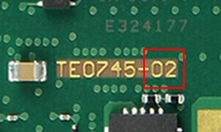
Figure 5: TE0745 SoC module revision number
Document Change History
| Date | Revision | Contributors | Description |
|---|---|---|---|
| 2017-03-31 | Ali Naseri, Jan Kumann | first First TRM release. | |
| 2017-02-05 | V1
| Jan Kumann | Initial document. |
...
Overview
Content Tools