Page History
...
The Trenz Electronic TE0745 is an industrial-grade SoC module integrating a Xilinx Zynq -7 SoC(ZXC7Z-7030030, ZXC7Z-7035 035 or ZXC7Z-7045045), 1 GByte DDR3/L SDRAM, 32 MByte SPI Flash memory for configuration and operation and powerful switch-mode power supplies for all on-board voltages. A large number of configurable I/O's is provided via rugged high-speed stacking strips.
...
Main Components
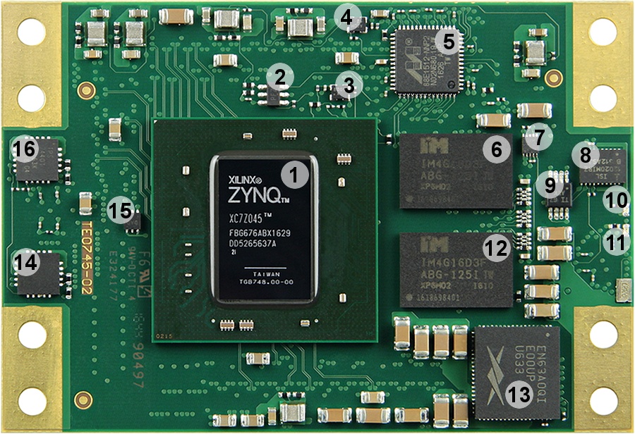
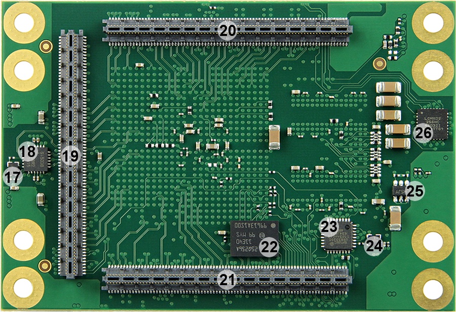
Figure 2: TE0745-02 SoC module
- Xilinx ZYNQ-7000 Zynq XC7Z family SoC, U1
- 256 Mbit Quad SPI Flash memory Micron N25Q256A, U12
- Reference clock signal oscillator SiTime SiT8008BI @33.333 MHz, U12
- Reference clock signal oscillator SiTime SiT8008BI @25.000 MHz, U9
- Marvell Alaska 88E1512 Gigabit Ethernet PHY, U3
- Intelligent Memory 512 MByte DDR3L-1600 SDRAM (8 Banks a 32 MWords, 16-bit word width), U3
- TI TPS51206 DDR3 memory termination regulator with buffered reference voltage VTTREF, U18
- Intersil ISL12020MIRZ Real-Time-Clock, U24
- TI TCA9517 level-shifting I2C bus repeater, U17
- Red LED, D2
- Green LED, D1
- Intelligent Memory 512 MByte DDR3L-1600 SDRAM (8 banks a 32 MWords, 16 Bit Word-Width), U5
- Altera Enpirion EN63A0QI 12A DC-DC PowerSoC @1.0V (VCCINT), U4
- TI TPS74401RGW LDO DC-DC regulator @1.2V (MGTAVTT), U8
- TI TPS72018DRVR LDO DC-DC regulator @1.8V (MGTAUX), U6
- TI TPS74401RGW LDO DC-DC regulator @1.0V (MGTAVCC), U11
- Silicon Labs Si5338A I2C Programmable Quad Clock Generator, U13
- Reference clock signal oscillator SiTime SiT8008BI @25.000 MHz, U21
- Samtec ST5-80-1.50-L-D-P-TR 160-pin stacking strips (2 rows a 80 positions), J3
- Samtec ST5-80-1.50-L-D-P-TR 160-pin stacking strips (2 rows a 80 positions), J1
- Samtec ST5-80-1.50-L-D-P-TR 160-pin stacking strips (2 rows a 80 positions), J2
- 256 Mbit Quad SPI Flash memory (Micron N25Q256A, U14
- Microchip USB3320 USB transceiver PHY , U32
- Reference clock signal oscillator SiTime SiT8008BI @52.000 MHz, U33
- Microchip 24AA025E48 EEPROM for MAC address, U23
- Lattice Semiconductor MachXO2-256HC System Controller CPLD, U2
...
Board to Board (B2B) I/O's
The Board to Board B2B connectors are high-speed hermaphroditic stacking strips and provide a modular interface to the SoC's PL and PS I/O's .The connector supports supporting single ended and differential signaling signalling as the I/O's Os are usable as LVDS pairs.
The I/O signals are routed from the SoC's PL banks as LVDS pairs to the B2B connectors.
| Bank | Type | B2B Connector | I/O Signal CountSignals | LVDS Pairs Count | VCCO Bank Voltage | Notes |
|---|---|---|---|---|---|---|
| 12 | HR | J1 | 50 | 24 | VCCIO_12 pins J1-54, J1-55 | supported voltages from Voltage range 1.2V to 3.3V |
| 13 | HR | J1 | 50 | 24 | VCCIO_13 pins J1-112, J1-113 | supported voltages from Voltage range 1.2V to 3.3V |
| 33 | HP | J3 | 50 | 24 | VCCIO_33 pins J3-115, J3-120 | supported voltages from 1Voltage range 1.2V to 1.8V |
| 34 | HP | J2 | 50 | 24 | VCCIO_34 pins J2-29, J2-30 | supported voltages from Voltage range 1.2V to 1.8V |
| 35 | HP | J2 | 50 | 24 | VCCIO_35 pins J2-87, J2-88 | supported voltages from 1Voltage range 1.2V to 1.8V |
| 500 | MIO | J2 | 5 | - | 1.8V | - |
| 501 | MIO | J3 | 12 | - | 1.8V | - |
Table 2: B2B connector pin-outs of available Count, type and voltage range of SoC's PL and PS banks of the SoC moduleI/O banks pins available through B2B connectors.
For detailed information about the pin-out, please refer to the Pin-out Table.
MGT Lanes
The B2B connector J1 and J2 provide also access to the MGT banks MGT bank signals of the SoC moduleare routed to the B2B connectors J1 and J3. There are 8 high-speed bi-directional data lanes (Xilinx GTX transceivertransceivers) available composed as differential signaling pairs for both directions (RX/TX). The MGT banks have On B2B connector J3 there are also clock input pins for MGT transceivers.
-pins which are exposed to the B2B connector J3. Following MGT lanes are available on the B2B connectors:
| Bank | Type | Lane Count | B2B Connector | Count of MGT Lanes | Schematic Schematics Names / Connector Pins | MGT Bank's Reference Clock Inputs (LVDS pairs) |
|---|---|---|---|---|---|---|
| Bank 111 | GTX | 4 | J1 | 4MGT_RX4_P, MGT MGT_RX4_N, pins J1-23, J1-21 MGT_RX5_P, MGT_RX5_N, pins J1-17, J1-15 MGT_RX6_P, MGT_RX6_N, pins J1-11, J1-9 MGT_RX7_P, MGT_RX7_N, pins J1-3, J1-5 | 1 reference Reference clock signal ( MGT_CLK3 ) from programmable 1 reference Reference clock signal ( MGT_CLK2 ) from B2B connector | |
| Bank 112 | GTX | 4 | J3 | 4 | MGT_RX3_P, MGT_RX3_N, pins J3-68, J3-70 MGT_RX2_P, MGT_RX2_N, pins J3-62, J3-64 MGT_RX1_P, MGT_RX1_N, pins J3-56, J3-58 MGT_RX0_P, MGT_RX0_N, pins J3-50, J3-52 | 1 reference clock signal (MGT_CLK1) from programmable 1 reference clock signal (MGT_CLK0) from B2B connector |
...
Table 5: B2B connector pin-out of SC CPLD I/O-pins
On-board LEDs
| LED | Color | connected Connected to | Description and Notes |
|---|---|---|---|
D1 | Green | SC System Controller CPLD, bank 3, pin 5 | System main status LED, blinking frequently or at system activity |
D2 | Red | Zynq -Chip chip (U1), bank 0 (config bank), 'DONE' (pin W9) | Reflects inverted DONE signal. ON when FPGA is not configured, OFF as soon as PL is configured. This LED will not operate if the SC System Controller CPLD can not power up the PL supply voltage. |
...
| Clock source | Schematic name | Frequency | Clock input destination | Note |
|---|---|---|---|---|
| B2B connector J3, pin pins J3-74/J3-76 | CLKIN_N, CLKIN_P | user | Quad PLL clock Generator generator U16, pin 1/2 | - |
| B2B connector J3, pin pins J3-75/J3-77 | MGT_CLK0_P, MGT_CLK0_N | user | MGT bank 112, pin R6/R5 | - |
| B2B connector J3, pin pins J3-81/J3-83 | MGT_CLK2_P, MGT_CLK2_N | user | MGT bank 111, pin W6/W5 | - |
| SiTime SiT8008BI oscillator, U21 | - | 25.000 000000 MHz | Quad PLL clock Generator generator U16, pin 3 | - |
SiTime SiT8008BI oscillator, U12 | PS_CLK | 33.333 333333 MHz | Bank 500 (MIO0 bank), pin B24 | - |
| SiTime SiT8008BI oscillator, U23 | OTG-RCLK | 52.000 000000 MHz | USB 2.0 Transceiver transceiver PHY U32, pin 26 | - |
| SiTime SiT8008BI oscillator, U9 | ETH_CLKIN | 25.000 000000 MHz | Gbit Ethernet PHY U7, pin 34 | - |
...
Overview
Content Tools