Page History
| Page properties | ||||
|---|---|---|---|---|
| ||||
Template Revision 2.3 |
| HTML |
|---|
<!--
Template Revision 1.68
(HTML comments will be not displayed in the document, no need to remove them. For Template/Skeleton changes, increase Template Revision number. So we can check faster, if the TRM style is up to date).
--> |
| HTML |
|---|
<!--
General Notes:
If some section is CPLD firmware dependent, make a note and if available link to the CPLD firmware description. It's in the TE shop download area in the corresponding module -> revision -> firmware folder.
--> |
| HTML |
|---|
<!--
General Notes:
Designate all graphics and pictures with a number and a description. For example "Figure 1: TE07xx-xx Block Diagram" or "Table 1: Initial delivery state". "Figure x" and "Table x" have to be formatted to bold.
--> |
| HTML |
|---|
<!--
Link to the base folder of the module (remove de/ or en/ from the URL): for example:
https://shop.trenz-electronic.de/Download/?path=Trenz_Electronic/Modules_and_Module_Carriers/4x5/4x5_Carriers/TE0703/
--> |
...
| Scroll pdf ignore | |
|---|---|
Table of Contents
|
Overview
The Trenz Electronic TEF1001 FPGA board is a PCI Express form factor card (PCIe 2.0 or higher) integrating the Xilinx Kintex-7 XC7K160T, XC7K325T or XC7K410T FPGA chip. The FPGA-board is designed for high system resources and intended for use in applications with high demands on system performance and throughput. The board offers a SO-DIMM socket on the board for standard DDR3 SDRAM extension memory module.
The board offers a HPC (High Pin Count) ANSI/VITA 57.1 compatible FMC interface connector for standard FPGA Mezzanine cards and modules. Other interface connectors found on-board include JTAG for accessing FPGA and on-board System Controller CPLD, and also connector with 5 high-speed I/O differential signaling pairs.
The TEF1001 FPGA board is intended to be used as add-on card in a PCIe 2.0 or higher capable host systems, it can not be used as a stand-alone device.
| HTML |
|---|
<!--
Use short link the Wiki resource page: for example:
http://trenz.org/tef1001-info
List of available short links: https://wiki.trenz-electronic.de/display/CON/Redirects
--> |
| Scroll Only (inline) |
|---|
Refer to http://trenz.org/tef1001-info for the current online version of this manual and other available documentation.
|
Key Features
List key features here, like FPGA type, amount and type of RAM, type of flash, etc.
Additional assembly options are available for cost or performance optimization upon request.
Block Diagram
| HTML |
|---|
<!--
Rules for all diagrams:
1. All diagrams are wrapped in the "Scroll Title" macro.
	- The title has to be named with the diagrams name
	- The anchor has the designation figure_x, whereby x is the number of the diagram

2. The Draw.IO diagram has to be inserted in the "Scroll Ignore" macro
	- Border has to be switched off in the macro edit
	- Toolbar has to be hidden in the macro edit

3. A PNG Export of the diagram has to be inserted in the "Scroll Only" macro, see Wiki page "Diagram Drawing Guidelines" how to do this step.

The workaround with the additional PNG of the diagram is necessary until the bug of the Scroll PDF Exporter, which cuts diagram to two pages, is fixed.


IMPORTANT NOTE: In case of copy and paste the TRM skeleton to a new Wiki page, delete the Draw.IO diagrams and the PNGs, otherwise due to the linkage of the copied diagrams every change in the TRM Skeleton will effect also in the created TRM and vice versa!

See page "Diagram Drawing Guidelines" how to clone an existing diagram as suitable template for the new diagram!

--> |
...
| anchor | Figure_1 |
|---|---|
| title | Figure 1: Example block diagram |
...
Main Components
Put top and bottom pics with labels of the real PCB here... like example diagram below
...
| anchor | Figure_2 |
|---|---|
| title | Figure 2: main components example diagram |
...
Table 1: TE0xxx-xx main components.
Add description list of PCB labels here...
Initial Delivery State
...
Storage device name
...
Content
...
Notes
...
..
...
..
...
Table 1: Initial delivery state of programmable devices on the module.
Boot Process
By default the ... supports QSPI and SD Card boot modes which is controlled by the MODE input signal from the B2B connector JM..
...
MODE Signal State
...
High or open
...
SD Card
...
Low or ground
...
QSPI Interface
Table 2: Selecting power-on boot device.
Signals, Interfaces and Pins
| HTML |
|---|
<!--
Connections and Interfaces or B2B Pin's which are accessible by User
--> |
Board to Board (B2B) I/Os
I/O signals connected to the SoCs I/O bank and B2B connector:
...
Table x: General overview of PL I/O signals connected to the B2B connectors.
All PS MIO banks are powered by on-module DC-DC power rail. All PL I/O banks have separate VCCO input pins in the B2B connectors, valid VCCO should be supplied from the carrier board.
For detailed information about the pin out, please refer to the Pin-out Tables.
The configuration of the PS I/Os MIOx, MIOx ... MIOx, ... depend on the carrier board peripherals connected to these pins.
| HTML |
|---|
<!--
TO-DO (future):
If Vivado board part files are available for this module, the standard configuration of the MIO pins by using this board part files should be mentioned here. This standard configuration of those pins are also apparent of the on-board peripherals of base-boards related to the module.
--> |
MGT Lanes
| HTML |
|---|
<!--
MGT lanes should be listed separately, as they are more specific than just general I/Os.
--> |
MGT (Multi Gigabit Transceiver) lane consists of one transmit and one receive (TX/RX) differential pairs, two signals each or four signals total per one MGT lane. Following table lists lane number, MGT bank number, transceiver type, signal schematic name, board-to-board pin connection and FPGA pins connection:
...
- MGT_RX0_P
- MGT_RX0_N
- MGT_TX0_P
- MGT_TX0_N
...
- JM3-8
- JM3-10
- JM3-7
- JM3-9
...
- MGTHRXP0_225, Y2
- MGTHRXN0_225, Y1
- MGTHTXP0_225, AA4
- MGTHTXN0_225, AA3
...
- MGT_RX1_P
- MGT_RX1_N
- MGT_TX1_P
- MGT_TX1_N
...
- JM3-14
- JM3-16
- JM3-13
- JM3-15
...
- MGTHRXP1_225, V2
- MGTHRXN1_225, V1
- MGTHTXP1_225, W4
- MGTHTXN1_225, W3
...
- MGT_RX4_P
- MGT_RX4_N
- MGT_TX4_P
- MGT_TX4_N
...
- JM1-12
- JM1-10
- JM1-6
- JM1-4
...
- MGTHRXP0_224, AH2
- MGTHRXN0_224, AH1
- MGTHTXP0_224, AG4
- MGTHTXN0_224, AG3
...
- MGT_RX5_P
- MGT_RX5_N
- MGT_TX5_P
- MGT_TX5_N
...
- JM1-24
- JM1-22
- JM1-18
- JM1-16
...
- MGTHRXP1_224, AF2
- MGTHRXN1_224, AF1
- MGTHTXP1_224, AF6
- MGTHTXN1_224, AF5
...
Table x: MGT lanes.
Below are listed MGT banks reference clock sources.
...
Table x: MGT reference clock sources.
JTAG Interface
JTAG access to the ... is provided through B2B connector ....
...
JTAG Signal
...
B2B Connector Pin
...
Table 5: JTAG interface signals.
System Controller CPLD I/O Pins
Special purpose pins are connected to smaller System Controller CPLD and have following default configuration:
...
Table x: System Controller CPLD I/O pins.
| HTML |
|---|
<!--
For the detailed function of the pins and signals, the internal signal assignment and implemented logic, look to the Wiki reference page SC CPLD of this module or into the bitstream file of the SC CPLD.
Add link to the Wiki reference page of the SC CPLD, if available.
--> |
Quad SPI Interface
Following line is just an example, change it to your needs.
Quad SPI Flash (U14) is connected to the Zynq PS QSPI0 interface via PS MIO bank 500, pins MIO1 ... MIO6.
Note that table column says "Signal Name", it should match the name used on the schematic.
...
Table x: Quad SPI interface signals and connections.
SD Card Interface
Describe SD Card interface shortly here if the module has one...
...
Table x: SD Card interface signals and connections.
Ethernet Interface
On board Gigabit Ethernet PHY is provided with ...
Ethernet PHY connection
...
Table x: ...
USB Interface
USB PHY is provided with ...
...
Table x: ...
The schematic for the USB connector and required components is different depending on the USB usage. USB standard A or B connectors can be used for Host or Device modes. A Mini USB connector can be used for USB Device mode. A USB Micro connector can be used for Device mode, OTG Mode or Host Mode.
I2C Interface
On-board I2C devices are connected to MIO.. and MIO.. which are configured as I2C... by default. I2C addresses for on-board devices are listed in the table below:
...
Table x: I2C slave device addresses.
On-board Peripherals
| HTML |
|---|
<!--
Components on the Module, like Flash, PLL, PHY...
--> |
System Controller CPLD
The System Controller CPLD (U2) is provided by Lattice Semiconductor LCMXO2-256HC (MachXO2 Product Family). The SC-CPLD is the central system management unit where essential control signals are logically linked by the implemented logic in CPLD firmware, which generates output signals to control the system, the on-board peripherals and the interfaces. Interfaces like JTAG and I2C between the on-board peripherals and to the FPGA module are by-passed, forwarded and controlled by the System Controller CPLD.
Other tasks of the System Controller CPLD are the monitoring of the power-on sequence and to display the programming state of the FPGA module.
For detailed information, refer to the reference page of the SC CPLD firmware of this module.
| HTML |
|---|
<!--
Put in link to the Wiki reference page of the firmware of the SC CPLD.
--> |
DDR Memory
By default TE0xxx module has ... DDRx SDRAM chips arranged into 32-bit wide memory bus providing total of 1 GBytes of on-board RAM. Different memory sizes are available optionally.
Quad SPI Flash Memory
On-board QSPI flash memory (U14) on the TE0745-02 is provided by Micron Serial NOR Flash Memory N25Q256A with 256 Mbit (32 MByte) storage capacity. This non volatile memory is used to store initial FPGA configuration. Besides FPGA configuration, remaining free flash memory can be used for user application and data storage. All four SPI data lines are connected to the FPGA allowing x1, x2 or x4 data bus widths. Maximum data rate depends on the selected bus width and clock frequency used.
| Note |
|---|
SPI Flash QE (Quad Enable) bit must be set to high or FPGA is unable to load its configuration from flash during power-on. By default this bit is set to high at the manufacturing plant. |
Gigabit Ethernet PHY
On-board Gigabit Ethernet PHY (U7) is provided with Marvell Alaska 88E1512 IC (U8). The Ethernet PHY RGMII interface is connected to the Zynq Ethernet0 PS GEM0. I/O voltage is fixed at 1.8V for HSTL signaling. The reference clock input of the PHY is supplied from an on-board 25.000000 MHz oscillator (U9), the 125MHz output clock signal CLK_125MHZ is connected to the pin J2-150 of B2B connector J2.
High-speed USB ULPI PHY
Hi-speed USB ULPI PHY (U32) is provided with USB3320 from Microchip. The ULPI interface is connected to the Zynq PS USB0 via MIO28..39, bank 501 (see also section). The I/O voltage is fixed at 1.8V and PHY reference clock input is supplied from the on-board 52.000000 MHz oscillator (U33).
MAC Address EEPROM
A Microchip 24AA025E48 serial EEPROM (U23) contains a globally unique 48-bit node address, which is compatible with EUI-48(TM) specification. The device is organized as two blocks of 128 x 8-bit memory. One of the blocks stores the 48-bit node address and is write protected, the other block is available for application use. It is accessible over I2C bus with slave device address 0x53.
RTC - Real Time Clock
An temperature compensated Intersil ISL...
Programmable Clock Generator
There is a Silicon Labs I2C programmable quad PLL clock generator on-board (Si5338A, U2) to generate various reference clocks for the module.
...
IN1
...
-
...
Not used.
...
IN3
...
Reference input clock.
...
IN4
...
IN5
...
-
...
CLK0A
...
CLK1_P
...
FPGA bank 45.
...
CLK0_P
...
FPGA bank 45.
...
Table : Programmable quad PLL clock generator inputs and outputs.
Oscillators
The module has following reference clock signals provided by on-board oscillators and external source from carrier board:
...
Table : Reference clock signals.
On-board LEDs
...
Table : On-board LEDs.
Power and Power-On Sequence
| HTML |
|---|
<!--
If power sequencing and distribution is not so much, you can join both sub sections together
--> |
Power Consumption
The maximum power consumption of a module mainly depends on the design running on the FPGA.
Xilinx provide a power estimator excel sheets to calculate power consumption. It's also possible to evaluate the power consumption of the developed design with Vivado. See also Trenz Electronic Wiki FAQ.
...
Table : Typical power consumption.
* TBD - To Be Determined soon with reference design setup.
Power supply with minimum current capability of ...A for system startup is recommended.
For the lowest power consumption and highest efficiency of the on-board DC-DC regulators it is recommended to power the module from one single 3.3V supply. All input power supplies have a nominal value of 3.3V. Although the input power supplies can be powered up in any order, it is recommended to power them up simultaneously.
The on-board voltages of the TE07xx SoC module will be powered-up in order of a determined sequence after the external voltages '...', '...' and '...' are available. All those power-rails can be powered up, with 3.3V power sources, also shared. <-- What?
| Warning |
|---|
| To avoid any damage to the module, check for stabilized on-board voltages should be carried out(i.e. power good and enable signals) before powering up any SoC's I/O bank voltages VCCO_x. All I/Os should be tri-stated during power-on sequence. |
Power Distribution Dependencies
Regulator dependencies and max. current.
Put power distribution diagram here...
Figure : Module power distribution diagram.
See Xilinx data sheet ... for additional information. User should also check related base board documentation when intending base board design for TE07xx module.
Power-On Sequence
The TE07xx SoM meets the recommended criteria to power up the Xilinx Zynq MPSoC properly by keeping a specific sequence of enabling the on-board DC-DC converters dedicated to the particular functional units of the Zynq chip and powering up the on-board voltages.
Following diagram clarifies the sequence of enabling the particular on-board voltages, which will power-up in descending order as listed in the blocks of the diagram:
Put power-on diagram here...
Figure : Module power-on diagram.
Voltage Monitor Circuit
If the module has one, describe it here...
Power Rails
NB! Following table with examples is valid for most of the 4 x 5 cm modules but depending on the module model and specific design, number and names of power rails connected to the B2B connectors may vary.
...
Power Rail Name
...
B2B JM1 Pins
...
B2B JM2 Pins
...
Direction
...
VBAT_IN
...
Table : Module power rails.
Different modules (not just 4 x 5 cm ones) have different type of connectors with different specifications. Following note is for Samtec Razor Beam™ LSHM connectors only, but we should consider adding such note into included file in Board to Board Connectors section instead of here.
| Note |
|---|
Current rating of Samtec Razor Beam™ LSHM B2B connectors is 2.0A per pin (2 adjacent pins powered). |
Bank Voltages
...
Bank
...
Voltage
...
Voltage Range
...
Table : Module PL I/O bank voltages.
Board to Board Connectors
| HTML |
|---|
<!--
Generate new entry:
Replace with correct on for selected module series
--> |
...
 tables have all same width (web max 1200px and pdf full page(640px), flexible width or fix width on menu for single column can be used as before) -->
<style>
.wrapped{
  width: 100% !important;
  max-width: 1200px !important;
 }
</style> |
| Page properties | ||||||||||||||||||||||||||||||||||||||||
|---|---|---|---|---|---|---|---|---|---|---|---|---|---|---|---|---|---|---|---|---|---|---|---|---|---|---|---|---|---|---|---|---|---|---|---|---|---|---|---|---|
| ||||||||||||||||||||||||||||||||||||||||
Important General Note:
|
| Page properties | ||||
|---|---|---|---|---|
| ||||
----------------------------------------------------------------------- |
| Page properties | ||||
|---|---|---|---|---|
| ||||
Note for Download Link of the Scroll ignore macro:
|
| Scroll Ignore |
|---|
| Scroll pdf ignore | |
|---|---|
Table of Contents
|
Overview
| Page properties | ||||
|---|---|---|---|---|
| ||||
Notes :
|
The Trenz Electronic TEF1001 FPGA board is a PCI Express form factor card integrating the Xilinx Kintex-7 XC7K160T, XC7K325T or XC7K410T FPGA SoC. The FPGA-board is designed for high system resources and intended for use in applications with high demands on system performance and throughput. To extent the board with standard DDR3 SDRAM memory module, there is a 204-pin SODIMM socket with 64bit databus width on the board present. Highspeed data transmission is enabled by the 4 lane PCIe Gen 2 interface.
The board offers a HPC (High Pin Count) ANSI/VITA 57.1 compatible FMC interface connector for standard FPGA Mezzanine cards and modules. Other interface connectors found on-board include JTAG for accessing FPGA and on-board System Controller CPLD.
The TEF1001 FPGA board is intended to be used as add-on card in a PCIe 2.0 or higher capable host system to meet the power supply requirements.
Refer to http://trenz.org/tef1001-info for the current online version of this manual and other available documentation.
Key Features
| Page properties | ||||
|---|---|---|---|---|
| ||||
Notes:
|
- Xilinx Kintex-7 XC7K160T, XC7K325T or XC7K410T FPGA SoC
- Large number of configurable I/Os are provided via HPC FMC connector
- 4 GTX high-performance transceiver
- 2x MGT transceiver clock inputs
- 160 FPGA I/O's (80 LVDS pairs)
- On-board high-efficiency switch-mode DC-DC converters
- Lattice MachXO2 LCMXO2-1200HC System Controller CPLD
- 10x User LEDs
- PCI Express x8 connector with 4 lane PCIe Gen 2 interface
- ANSI Vita 57.1 FMC High Pin Count (HPC) connector
- DDR3 SODIMM SDRAM with ECC socket with 64bit databus width
- 256Mbit (32MByte) Quad SPI Flash memory (for configuration and operation) accessible through:
- FPGA
- JTAG port (SPI indirect, bus width x4)
- FPGA configuration through:
- JTAG connector
- Quad SPI Flash memory
Clocking
Si5338 programmable quad PLL clock generator - 4 outputs for MGT and PL clocks
200MHz oscillator for DDR3 bank
- System management and power sequencing
Additional assembly options are available for cost or performance optimization upon request.
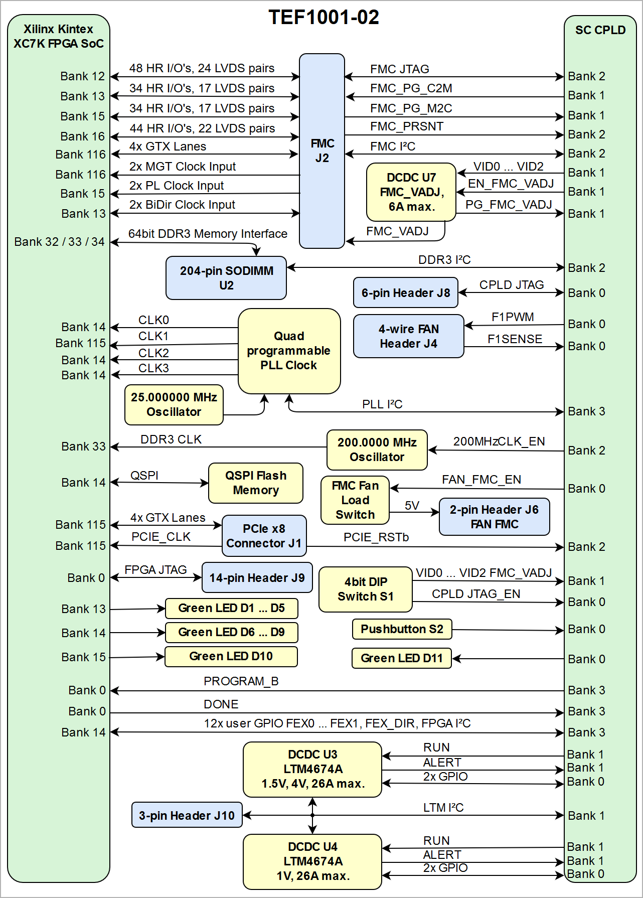
Block Diagram
| Scroll Title | ||||||||||||||||||||||||||||||||
|---|---|---|---|---|---|---|---|---|---|---|---|---|---|---|---|---|---|---|---|---|---|---|---|---|---|---|---|---|---|---|---|---|
| ||||||||||||||||||||||||||||||||
|
Main Components
| Page properties | ||||
|---|---|---|---|---|
| ||||
Notes :
|
| Scroll Title | ||||||||||||||||||||||||||||||||
|---|---|---|---|---|---|---|---|---|---|---|---|---|---|---|---|---|---|---|---|---|---|---|---|---|---|---|---|---|---|---|---|---|
| ||||||||||||||||||||||||||||||||
|
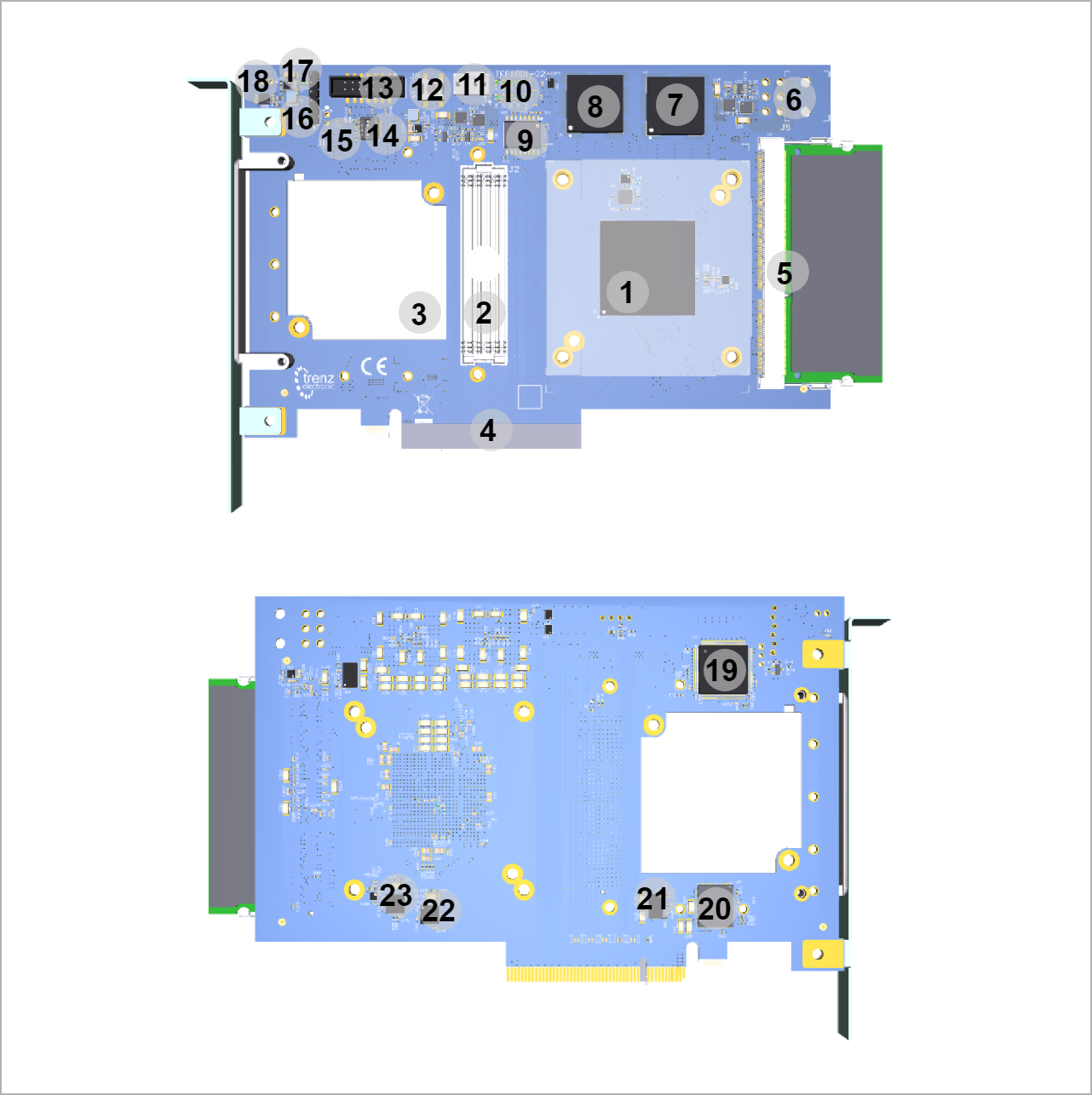
- Xilinx Kintex XC7K-2FBG676I FPGA SoC, U6
- ANSI/VITA 57.1 compliant FMC HPC connector, J2
- Cooling fan 5VDC M1 (45X5MM, 0.7W, 1.06CFM), M1
- PCIe x8 connector, J1
- DDR3 SODIMM 204-pin socket, U2
- 6-pin 12V power connector, J5
- Step-down DC-DC converter @1.5V and @4V (LT LTM4676A), U3
- Step-down DC-DC converter @1.0V (LT LTM4676A), U4
- 256 Mbit Quad SPI Flash Memory (Micron N25Q256A), U12
- 10x Green user LEDs connected to FPGA, D1 ... D10
- 4-wire PWM fan connector, J4
- User button, S2
- FPGA JTAG connector, J9
- 4bit DIP switch, S1
- I²C header for LTM4676A DC-DC converter, J10
- System Controller CPLD JTAG header, J8
- 1x Green LED connected to SC CPLD, D11
- 2-pin 5V FAN header, J6
- System Controller CPLD (Lattice Semiconductor LCMXO2-1200HC), U5
- 6A PowerSoC DC-DC converter @FMC_VADJ (Altera EN5365QI), U7
- 4A PowerSoC DC-DC converter @3.3V (3V3FMC) (Altera EN6347QI), U15
- LDO converter @1.2V (MGTAVTT_FPGA) (TI TPS74401RGW), U17
- LDO converter @1.0V (MGTAVCC_FPGA) (TI TPS74401RGW), U18
- 4A PowerSoC DC-DC converter @1.8V (Altera EN6347QI), U7
Initial Delivery State
| Scroll Title | ||||||||||||||||||||||||||||||||||||||||||
|---|---|---|---|---|---|---|---|---|---|---|---|---|---|---|---|---|---|---|---|---|---|---|---|---|---|---|---|---|---|---|---|---|---|---|---|---|---|---|---|---|---|---|
| ||||||||||||||||||||||||||||||||||||||||||
|
Control Signals
To get started with TEF1001 board, some basic control signals are essential and are described in the following table:
| Scroll Title | ||||||||||||||||||||||||||||||||||||||||||||||||
|---|---|---|---|---|---|---|---|---|---|---|---|---|---|---|---|---|---|---|---|---|---|---|---|---|---|---|---|---|---|---|---|---|---|---|---|---|---|---|---|---|---|---|---|---|---|---|---|---|
| ||||||||||||||||||||||||||||||||||||||||||||||||
|
Signals, Interfaces and Pins
| Page properties | ||||
|---|---|---|---|---|
| ||||
Notes:
|
FMC HPC Connector
I/O signals and interfaces connected to the FPGA SoCs I/O bank and FMC connector J2:
| Scroll Title | |||||||||||||||||||||||||||||||||||||||||||||||||||||||||||||||||||||||||
|---|---|---|---|---|---|---|---|---|---|---|---|---|---|---|---|---|---|---|---|---|---|---|---|---|---|---|---|---|---|---|---|---|---|---|---|---|---|---|---|---|---|---|---|---|---|---|---|---|---|---|---|---|---|---|---|---|---|---|---|---|---|---|---|---|---|---|---|---|---|---|---|---|---|
| |||||||||||||||||||||||||||||||||||||||||||||||||||||||||||||||||||||||||
|
For detailed information about the pin out, please refer to the Pin-out Tables.
FMC connector J2 MGT Lanes:
| Scroll Title | ||||||||||||||||||||||||||||||||||||||||||||||||
|---|---|---|---|---|---|---|---|---|---|---|---|---|---|---|---|---|---|---|---|---|---|---|---|---|---|---|---|---|---|---|---|---|---|---|---|---|---|---|---|---|---|---|---|---|---|---|---|---|
| ||||||||||||||||||||||||||||||||||||||||||||||||
|
FMC connector J2 reference clock sources:
| Scroll Title | |||||||||||||||||||||||||||||||||
|---|---|---|---|---|---|---|---|---|---|---|---|---|---|---|---|---|---|---|---|---|---|---|---|---|---|---|---|---|---|---|---|---|---|
| |||||||||||||||||||||||||||||||||
|
FMC connector J2 VCC/VCCIO:
| Scroll Title | ||||||||||||||||||||||||||||||||||||||
|---|---|---|---|---|---|---|---|---|---|---|---|---|---|---|---|---|---|---|---|---|---|---|---|---|---|---|---|---|---|---|---|---|---|---|---|---|---|---|
| ||||||||||||||||||||||||||||||||||||||
|
FMC connector J2 Cooling Fan:
| Scroll Title | ||||||||||||||||||||||||
|---|---|---|---|---|---|---|---|---|---|---|---|---|---|---|---|---|---|---|---|---|---|---|---|---|
| ||||||||||||||||||||||||
|
PCI Express Interface
The TEF1001 FPGA board is a PCI Express card designed to fit into systems with PCI Express x8 slots and has a data transmission capability which meets PCIe Gen. 2 with 4 GTX lanes routed to the PCIe interface.
Following table lists lane number, MGT bank number, transceiver type, signal schematic name, connector and FPGA pins connection:
| Scroll Title | ||||||||||||||||||||||||||||||||||||||||||||||||
|---|---|---|---|---|---|---|---|---|---|---|---|---|---|---|---|---|---|---|---|---|---|---|---|---|---|---|---|---|---|---|---|---|---|---|---|---|---|---|---|---|---|---|---|---|---|---|---|---|
| ||||||||||||||||||||||||||||||||||||||||||||||||
|
| Scroll Title | ||||||||||||||||||||||||||||||
|---|---|---|---|---|---|---|---|---|---|---|---|---|---|---|---|---|---|---|---|---|---|---|---|---|---|---|---|---|---|---|
| ||||||||||||||||||||||||||||||
|
JTAG Connectors
There are two JTAG connectors J8 and J9 available on the TEF1001 board:
| Scroll Title | ||||||||||||||||||||||||||||||||||||||||||||||||||||
|---|---|---|---|---|---|---|---|---|---|---|---|---|---|---|---|---|---|---|---|---|---|---|---|---|---|---|---|---|---|---|---|---|---|---|---|---|---|---|---|---|---|---|---|---|---|---|---|---|---|---|---|---|
| ||||||||||||||||||||||||||||||||||||||||||||||||||||
|
FAN Connectors
The TEF1001 board offers one FAN connector for cooling the FPGA device and one built-in FAN for the FMC modules.
| Scroll Title | ||||||||||||||||||||||||||||||
|---|---|---|---|---|---|---|---|---|---|---|---|---|---|---|---|---|---|---|---|---|---|---|---|---|---|---|---|---|---|---|
| ||||||||||||||||||||||||||||||
|
On-board Peripherals
| Page properties | ||||
|---|---|---|---|---|
| ||||
Notes :
|
System Controller CPLD
The System Controller CPLD (U5) is provided by Lattice Semiconductor LCMXO2-256HC (MachXO2 Product Family). The SC-CPLD is the central system management unit where essential control signals are logically linked by the implemented logic in CPLD firmware, which generates output signals to control the system, the on-board peripherals and the interfaces. Interfaces like JTAG and I2C between the on-board peripherals and to the FPGA module are by-passed, forwarded and controlled by the System Controller CPLD.
Other tasks of the System Controller CPLD are the monitoring of the power-on sequence and to display the programming state of the FPGA module.
For detailed function of the pins and signals, the internal signal assignment and the implemented logic, look to the Wiki reference page of the board's SC CPLD or into its bitstream file.. Table below lists the SC CPLD I/O pins with their default configuration:
| Scroll Title | ||||||||||||||||||||||||||||||||||||||||||||||||||||||||||||||||||||||||||||||||||||||||||||||||||||||||||||||||||||||||||||||||||||||||||||||||||||||||||||||||||||||||
|---|---|---|---|---|---|---|---|---|---|---|---|---|---|---|---|---|---|---|---|---|---|---|---|---|---|---|---|---|---|---|---|---|---|---|---|---|---|---|---|---|---|---|---|---|---|---|---|---|---|---|---|---|---|---|---|---|---|---|---|---|---|---|---|---|---|---|---|---|---|---|---|---|---|---|---|---|---|---|---|---|---|---|---|---|---|---|---|---|---|---|---|---|---|---|---|---|---|---|---|---|---|---|---|---|---|---|---|---|---|---|---|---|---|---|---|---|---|---|---|---|---|---|---|---|---|---|---|---|---|---|---|---|---|---|---|---|---|---|---|---|---|---|---|---|---|---|---|---|---|---|---|---|---|---|---|---|---|---|---|---|---|---|---|---|---|---|---|---|
| ||||||||||||||||||||||||||||||||||||||||||||||||||||||||||||||||||||||||||||||||||||||||||||||||||||||||||||||||||||||||||||||||||||||||||||||||||||||||||||||||||||||||
|
DDR3 SDRAM ECC SO-DIMM Socket
The TEF1001 board supports additional DDR3 ECC SO-DIMM via 204-pin socket U2. The DDR3 memory interface has a 64bit wide databus and is routed to the FPGA banks 32, 33 and 34.
The reference clock signal for the DDR3 interface is generated by the 200.0000MHz MEMS oscillator U1 and is applied to the FPGA bank 33.
There is also a I2C interface between the System Controller CPLD U5 and the DDR3 ECC SO-DIMM memory socket U2.
| Scroll Title | ||||||||||||||||||||||||||||
|---|---|---|---|---|---|---|---|---|---|---|---|---|---|---|---|---|---|---|---|---|---|---|---|---|---|---|---|---|
| ||||||||||||||||||||||||||||
|
| Info |
|---|
It is important to use SO-DIMMs which provide ECC functionality. SO-DIMMs without ECC are not compatible with this board. |
Quad SPI Flash Memory
A 256 Mbit (32 MByte) Quad SPI Flash Memory (Micron N25Q256A, U12) is provided for FPGA configuration file storage. After configuration process completes the remaining free memory can be used for application data storage. All four SPI data lines are connected to the FPGA allowing x1, x2 or x4 data bus widths to be used. The maximum data transfer rate depends on the bus width and clock frequency. The memory can be accessed indirectly by the FPGA JTAG port (J9) by implementing the functional logic for this purpose inside the FPGA.
Quad SPI Flash memory interface is connected to the FPGA bank 14, QSPI clock is provided by FPGA config bank 0.
| Scroll Title | |||||||||||||||||||||||||||||||||||||||
|---|---|---|---|---|---|---|---|---|---|---|---|---|---|---|---|---|---|---|---|---|---|---|---|---|---|---|---|---|---|---|---|---|---|---|---|---|---|---|---|
| |||||||||||||||||||||||||||||||||||||||
|
| Note |
|---|
SPI Flash QE (Quad Enable) bit must be set to high or FPGA is unable to load its configuration from flash during power-on. By default this bit is set to high at the manufacturing plant. |
Programmable Clock Generator
There is a Silicon Labs I2C programmable quad PLL clock generator on-board (Si5338A, U13) to generate various reference clocks for the module.
| Scroll Title | ||||||||||||||||||||||||||||||||||||||||||||||||||||||||||||||||||||||||||||||||||||||||||||||
|---|---|---|---|---|---|---|---|---|---|---|---|---|---|---|---|---|---|---|---|---|---|---|---|---|---|---|---|---|---|---|---|---|---|---|---|---|---|---|---|---|---|---|---|---|---|---|---|---|---|---|---|---|---|---|---|---|---|---|---|---|---|---|---|---|---|---|---|---|---|---|---|---|---|---|---|---|---|---|---|---|---|---|---|---|---|---|---|---|---|---|---|---|---|---|
| ||||||||||||||||||||||||||||||||||||||||||||||||||||||||||||||||||||||||||||||||||||||||||||||
|
Oscillators
The FPGA module has following reference clocking sources provided by on-board oscillators and FMC connector J2:
| Scroll Title | ||||||||||||||||||||||||||||||||||||||||||||||||||||||||||||||||||||||||
|---|---|---|---|---|---|---|---|---|---|---|---|---|---|---|---|---|---|---|---|---|---|---|---|---|---|---|---|---|---|---|---|---|---|---|---|---|---|---|---|---|---|---|---|---|---|---|---|---|---|---|---|---|---|---|---|---|---|---|---|---|---|---|---|---|---|---|---|---|---|---|---|---|
| ||||||||||||||||||||||||||||||||||||||||||||||||||||||||||||||||||||||||
|
On-board LEDs
| Scroll Title | |||||||||||||||||||||||||||||||||||||||||||||||||||||||||||||||||||||
|---|---|---|---|---|---|---|---|---|---|---|---|---|---|---|---|---|---|---|---|---|---|---|---|---|---|---|---|---|---|---|---|---|---|---|---|---|---|---|---|---|---|---|---|---|---|---|---|---|---|---|---|---|---|---|---|---|---|---|---|---|---|---|---|---|---|---|---|---|---|
| |||||||||||||||||||||||||||||||||||||||||||||||||||||||||||||||||||||
|
Configuration DIP-switch
There is one 4-bit DIP-witches S1 present on the TEB0911 board to configure options and set parameters. The following section describes the functionalities of the particular switches.
Table below describes the functionalities of the switches of DIP-switches S3 and S4 at their each positions:
| Scroll Title | |||||||||||||||||||||||||||||||||||||||
|---|---|---|---|---|---|---|---|---|---|---|---|---|---|---|---|---|---|---|---|---|---|---|---|---|---|---|---|---|---|---|---|---|---|---|---|---|---|---|---|
| |||||||||||||||||||||||||||||||||||||||
|
Push Buttons
There is one push buttons available to the user connected to the SC CPLD U5:
| Scroll Title | ||||||||||||||||||||||||||
|---|---|---|---|---|---|---|---|---|---|---|---|---|---|---|---|---|---|---|---|---|---|---|---|---|---|---|
| ||||||||||||||||||||||||||
|
Power and Power-On Sequence
Power Consumption
The maximum power consumption of a module mainly depends on the design running on the FPGA.
Xilinx provide a power estimator excel sheets to calculate power consumption. It's also possible to evaluate the power consumption of the developed design with Vivado. See also Trenz Electronic Wiki FAQ.
| Scroll Title | ||||||||||||||||||||||
|---|---|---|---|---|---|---|---|---|---|---|---|---|---|---|---|---|---|---|---|---|---|---|
| ||||||||||||||||||||||
|
* TBD - To Be Determined soon with reference design setup.
It is recommended to connect the ATX connector J5 to a 12V power supply source with minimum current capability of 6A to provide a sufficient power source to the board. Only one power source is needed at the same time, the system disconnects automatically PCIe power supply from PCIe edge connector J1 if the board is powered by the ATX connector J5.
| Warning |
|---|
| To avoid any damage to the module, check for stabilized on-board voltages should be carried out (i.e. power good and enable signals) before powering up any FPGA's I/O bank voltages VCCO_x. All I/Os should be tri-stated during power-on sequence. |
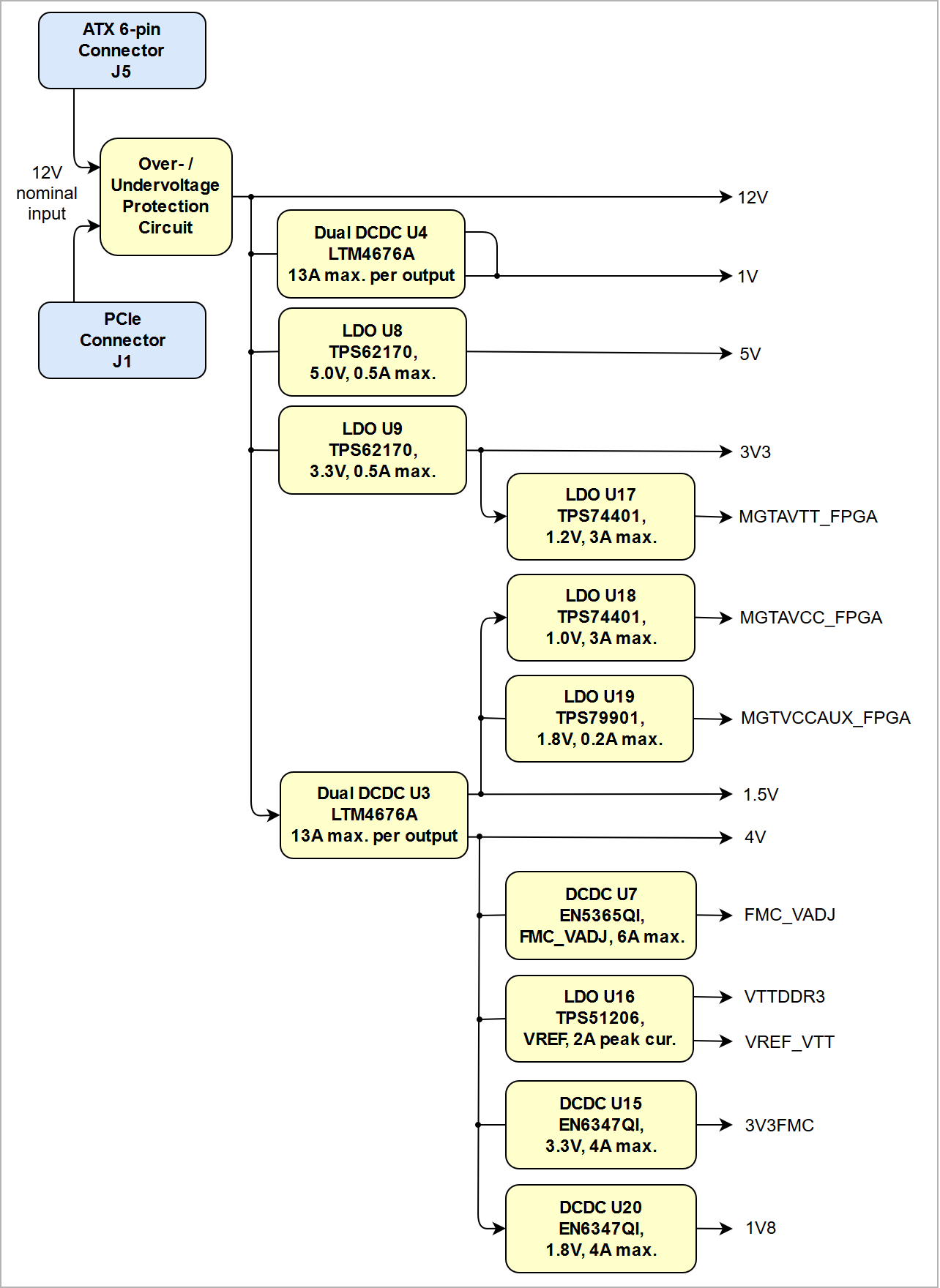
Power Distribution Dependencies
| Scroll Title | ||||||||||||||||||||||||||||||||
|---|---|---|---|---|---|---|---|---|---|---|---|---|---|---|---|---|---|---|---|---|---|---|---|---|---|---|---|---|---|---|---|---|
| ||||||||||||||||||||||||||||||||
|
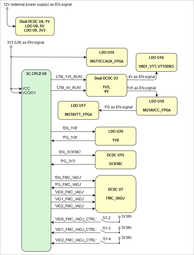
Power-On Sequence
The TEF1001 board meets the recommended criteria to power up the Xilinx FPGA properly by keeping a specific sequence of enabling the on-board DC-DC converters dedicated to the particular functional units of the FPGA chip and powering up the on-board voltages.
Some of the voltages are handled by the System Controller CPLD using "Power good"-signals from the voltage regulators:
Following diagram clarifies the sequence of enabling the particular on-board voltages, which will power-up in descending order as listed in the blocks of the diagram:
| Scroll Title | ||||||||||||||||||||||||||||||||
|---|---|---|---|---|---|---|---|---|---|---|---|---|---|---|---|---|---|---|---|---|---|---|---|---|---|---|---|---|---|---|---|---|
| ||||||||||||||||||||||||||||||||
|
Bank Voltages
| Scroll Title | |||||||||||||||||||||||||||||||||||||||||||||||||||||||||||||||||||||||||
|---|---|---|---|---|---|---|---|---|---|---|---|---|---|---|---|---|---|---|---|---|---|---|---|---|---|---|---|---|---|---|---|---|---|---|---|---|---|---|---|---|---|---|---|---|---|---|---|---|---|---|---|---|---|---|---|---|---|---|---|---|---|---|---|---|---|---|---|---|---|---|---|---|---|
| |||||||||||||||||||||||||||||||||||||||||||||||||||||||||||||||||||||||||
|
Power Rails
| Scroll Title | ||||||||||||||||||||||||||||||||||||||||||||||||||||||||||||||||||||||||||
|---|---|---|---|---|---|---|---|---|---|---|---|---|---|---|---|---|---|---|---|---|---|---|---|---|---|---|---|---|---|---|---|---|---|---|---|---|---|---|---|---|---|---|---|---|---|---|---|---|---|---|---|---|---|---|---|---|---|---|---|---|---|---|---|---|---|---|---|---|---|---|---|---|---|---|
| ||||||||||||||||||||||||||||||||||||||||||||||||||||||||||||||||||||||||||
|
Technical Specifications
Absolute Maximum Ratings
| Scroll Title | |||||||||||||||||||||||||||||||||||||||||||||||||||||||||||||||||||||||||||||||||||
|---|---|---|---|---|---|---|---|---|---|---|---|---|---|---|---|---|---|---|---|---|---|---|---|---|---|---|---|---|---|---|---|---|---|---|---|---|---|---|---|---|---|---|---|---|---|---|---|---|---|---|---|---|---|---|---|---|---|---|---|---|---|---|---|---|---|---|---|---|---|---|---|---|---|---|---|---|---|---|---|---|---|---|---|
| |||||||||||||||||||||||||||||||||||||||||||||||||||||||||||||||||||||||||||||||||||
|
| Note |
|---|
| Assembly variants for higher storage temperature range are available on request. |
Recommended Operating Conditions
| Scroll Title | ||||||||||||||||||||||||||||||||||||||||||||||||||||||||||||||||||||
|---|---|---|---|---|---|---|---|---|---|---|---|---|---|---|---|---|---|---|---|---|---|---|---|---|---|---|---|---|---|---|---|---|---|---|---|---|---|---|---|---|---|---|---|---|---|---|---|---|---|---|---|---|---|---|---|---|---|---|---|---|---|---|---|---|---|---|---|---|
| ||||||||||||||||||||||||||||||||||||||||||||||||||||||||||||||||||||
|
1) Temperature range may vary depending on assembly options
2) The operating temperature range of the FPGA soC and on-board peripherals are junction and also ambient operating temperature ranges
Board operating temperature range depends also on customer design and cooling solution. Please contact us for options.
| Note |
|---|
| Please check also Xilinx datasheet DS182 for complete list of absolute maximum and recommended operating ratings. |
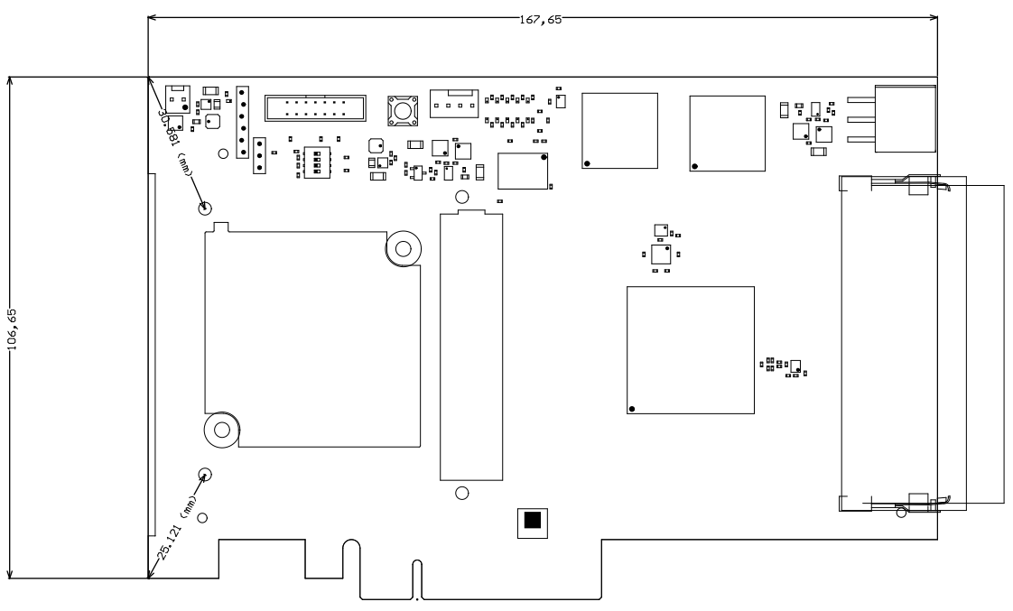
Physical Dimensions
| Scroll Title | ||||
|---|---|---|---|---|
| ||||
|
Variants Currently In Production
| Page properties | ||||
|---|---|---|---|---|
| ||||
|
| Scroll Title | ||||||||||||||||||||||
|---|---|---|---|---|---|---|---|---|---|---|---|---|---|---|---|---|---|---|---|---|---|---|
| ||||||||||||||||||||||
| ||||||||||||||||||||||
Revision History
Hardware Revision History
| Scroll Title | |||||||||||||||||||||||||||||||||
|---|---|---|---|---|---|---|---|---|---|---|---|---|---|---|---|---|---|---|---|---|---|---|---|---|---|---|---|---|---|---|---|---|---|
| |||||||||||||||||||||||||||||||||
|
| Scroll Title | ||||
|---|---|---|---|---|
| ||||
|
Hardware revision number can be found on the PCB board together with the module model number separated by the dash.
Document Change History
| Page properties | ||||
|---|---|---|---|---|
| ||||
|
| Scroll Title | ||||||||||||||||||||||||||||||||||||||||||||||||||||||||
|---|---|---|---|---|---|---|---|---|---|---|---|---|---|---|---|---|---|---|---|---|---|---|---|---|---|---|---|---|---|---|---|---|---|---|---|---|---|---|---|---|---|---|---|---|---|---|---|---|---|---|---|---|---|---|---|---|
| ||||||||||||||||||||||||||||||||||||||||||||||||||||||||
|
...
Variants Currently In Production
| HTML |
|---|
<!--
Set correct link to the overview table of the product on english and german, if not available, set
https://shop.trenz-electronic.de/de/Produkte/Trenz-Electronic/
https://shop.trenz-electronic.de/en/Products/Trenz-Electronic/
--> |
...
Technical Specifications
Absolute Maximum Ratings
...
Parameter
...
Units
...
Reference Document
...
VIN supply voltage
...
V
...
Storage temperature
...
°C
...
Table : Module absolute maximum ratings.
| Note |
|---|
| Assembly variants for higher storage temperature range are available on request. |
Recommended Operating Conditions
...
Table : Module recommended operating conditions.
| Note |
|---|
| Please check Xilinx datasheet ... for complete list of absolute maximum and recommended operating ratings. |
Operating Temperature Ranges
Commercial grade: 0°C to +70°C.
Extended grade: 0°C to +85°C.
Industrial grade: -40°C to +85°C.
Module operating temperature range depends also on customer design and cooling solution. Please contact us for options.
Physical Dimensions
Module size: ... mm × ... mm. Please download the assembly diagram for exact numbers.
Mating height with standard connectors: ... mm.
PCB thickness: ... mm.
Highest part on PCB: approx. ... mm. Please download the step model for exact numbers.
All dimensions are given in millimeters.
Put mechanical drawings here...
Figure : Module physical dimensions drawing.
Revision History
Hardware Revision History
...
Notes
...
01
...
Prototypes
Table : Module hardware revision history.
Hardware revision number can be found on the PCB board together with the module model number separated by the dash.
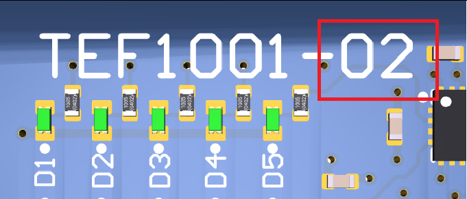
Put picture of actual PCB showing model and hardware revision number here...
Figure : Module hardware revision number.
Document Change History
| HTML |
|---|
<!--
Generate new entry:
1.add new row below first
2.Copy "Page Information Macro(date)" Macro-Preview, Metadata Version number, Author Name and description to the empty row. Important Revision number must be the same as the Wiki document revision number
3.Update Metadata = "Page Information Macro (current-version)" Preview+1 and add Author and change description.
--> |
...
Date
...
Revision
...
Contributors
...
Description
...
| Page info | ||||||||
|---|---|---|---|---|---|---|---|---|
|
...
- updated rules for draw.IO diagram
...
- Added new rule for draw.IO diagram with workaround for "Scroll PDF Exporter"
...
...
- nothing new (recreated destroyed document)
...
2018-05-09
...
v.63
...
- Rework chapter currently available products
...
...
- Remove Link to Download
...
v.58...
- PDF-Link to online version of the TRM fixed
- Online Link of download area fixed
...
2017-09-06
...
v.56
...
2017-09-02
...
v.54
...
2017-08-27
...
v.43
...
- New template revision 1.6.
- Moved Boot Process between Overview and Signals, Interfaces and Pins section.
...
- New template revision 1.5
- MGT Lanes section changed.
- Programmable PLL Clock section changed.
- "Figure" and "Table" labels added.
- Module variants and temperatures ranges sections improved.
- Comments added/changed, also formatted as italic now.
...
2017-08-07
...
v.32
...
2017-07-14
...
v.25
...
John Hartfiel
...
Removed weight section update template version
...
2017-06-08
...
v.20
...
John Hartfiel
...
Add revision number and update document change history
...
2017-05-30
...
v.1
...
Jan Kumann
...
Initial document.
Table : Document change history.
Disclaimer
| Include Page | ||||
|---|---|---|---|---|
|
Overview
Content Tools