Page History
...
- Xilinx Zynq XC7Z family SoC, U1
- 256 Mbit Quad SPI Flash memory Micron N25Q256A, U12
- Reference clock signal oscillator SiTime SiT8008BI @33.333333 MHz, U12
- Reference clock signal oscillator SiTime SiT8008BI @25.000000 MHz, U9
- Marvell Alaska 88E1512 Gigabit Ethernet PHY, U3
- Intelligent Memory 512 MByte DDR3L-1600 SDRAM (8 Banks a 32 MWords, 16-bit word width), U3
- TI TPS51206 DDR3 memory termination regulator with buffered reference voltage VTTREF, U18
- Intersil ISL12020MIRZ Real-Time-Clock, U24
- TI TCA9517 level-shifting I2C bus repeater, U17
- Red LED, D2
- Green LED, D1
- Intelligent Memory 512 MByte DDR3L-1600 SDRAM (8 banks a 32 MWords, 16 Bit word width), U5
- Altera Enpirion EN63A0QI 12A DC-DC PowerSoC @1.0V (VCCINT), U4
- TI TPS74401RGW LDO DC-DC regulator @1.2V (MGTAVTT), U8
- TI TPS72018DRVR LDO DC-DC regulator @1.8V (MGTAUX), U6
- TI TPS74401RGW LDO DC-DC regulator @1.0V (MGTAVCC), U11
- Silicon Labs Si5338A I2C Programmable Quad Clock Generator, U13
- Reference clock signal oscillator SiTime SiT8008BI @25.000 MHz, U21
- Samtec ST5-80-1.50-L-D-P-TR 160-pin stacking strips (2 rows a 80 positions), J3
- Samtec ST5-80-1.50-L-D-P-TR 160-pin stacking strips (2 rows a 80 positions), J1
- Samtec ST5-80-1.50-L-D-P-TR 160-pin stacking strips (2 rows a 80 positions), J2
- 256 Mbit Quad SPI Flash memory (Micron N25Q256A), U14
- Microchip USB3320 USB transceiver PHY , U32
- Reference clock signal oscillator SiTime SiT8008BI @52.000000 MHz, U33
- Microchip 24AA025E48 EEPROM for MAC address, U23
- Lattice Semiconductor MachXO2-256HC System Controller CPLD, U2
...
The on-board voltages of the TE0745 SoC module will be powered-up in order of a determined sequence after the external voltages 'PL_VIN', 'PS_VIN' and 'PS_3.3V' are available. All those power-rails can be powered up, with 3.3V power sources, also shared.
| Warning |
|---|
| To avoid any damage to the SoC module, check for stabilized on-board voltages in steady state before powering up the SoC's I/O bank voltages VCCO_x. |
...
It is important that all baseboard I/Os are 3-stated at power-on until the "Power Good"-signals 'PWR_PS_OK' (J2-139) and 'PWR_PL_OK' (J2-135) are high, meaning that all on-module voltages have become stable and module is properly powered up.
Following diagram clarifies the sequence of enabling There are following dependencies how the initial voltages of the power rails on the B2B connectors are distributed to the on-board DCDC converters, which power up further DCDC converters and the particular on-board voltages:
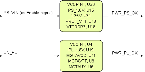
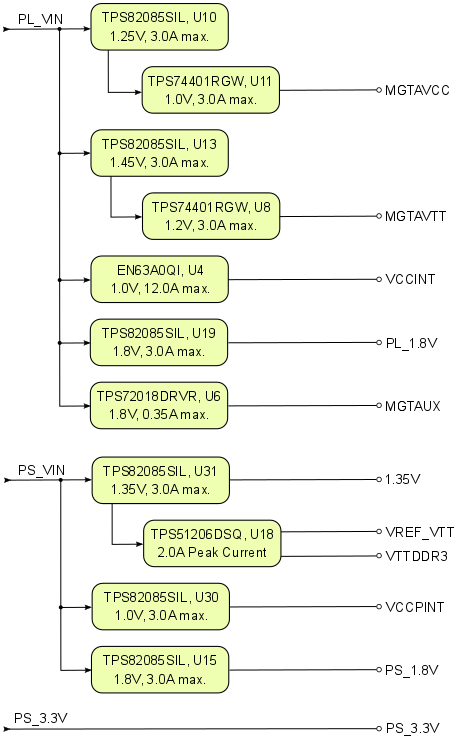
Figure 3: Power -up sequence diagramDistribution Diagram
See Xilinx datasheet data sheet DS191 for additional information. User should also check related base board documentation when intending base board design for TE0745 module.
Power
...
-On Sequence Diagram
The TE0745 SoM meets the recommended criteria to power up the Xilinx Zynq MPSoC properly by keeping a specific sequence of enabling the on-board DCDC converters dedicated to the particular functional units of the Zynq chip and powering up the on-board voltages.
Following diagram clarifies the sequence of enabling the particular on-board voltages, which will power-up in descending order as listed in the blocks of the diagram:
Figure 4: Power-On Sequence
The Enable-Signal 'EN_PL' is permanently logic high in standard SC-CPLD firmware. The "Power Good"-signals 'PWR_PS_OK' and 'PWR_PL_OK' (latter low-active, extern pull-up needed) are available B2B-connector J2 (pins J2-139, J2-135) and on the SC-CPLD.
Power Rails
Voltages on B2B | Voltages on B2B | B2B J1 Pin | B2B J2 Pin | B2B J3 Pin | Input/ | Note |
|---|---|---|---|---|---|---|
| PL_VIN | 147, 149, 151, 153, | - | - | Input | supply voltage | |
| PS_VIN | - | 154, 156, 158 | - | Input | supply voltage | |
| PS_3.3V | - | 160 | - | Input | supply voltage | |
| VCCIO12 | 54, 55 | - | - | Input | high range bank I/O voltage | |
| VCCIO13 | 112, 113 | - | - | Input | high range bank I/O voltage | |
| VCCIO33 | - | - | 115, 120 | Input | high performance bank I/O voltage | |
| VCCIO34 | 29, 30 | - | Input | high performance bank I/O voltage | ||
| VCCIO35 | 87, 88 | - | Input | high performance bank I/O voltage | ||
| VBAT_IN | 146 | - | - | Input | RTC (battery-backed) supply voltage | |
| PS_1.8V | - | 130 | - | Output | internal 1.8V voltage level (Process System supply) |
...
Table 17: Differences between variants of Module TE0808TE0745-0402
Technical Specification
Absolute Maximum Ratings
Parameter | Min | Max | Units | Notes |
|---|---|---|---|---|
| PL_VIN | -0.3 | 5 | V | TI TPS720 data sheet |
| PS_VIN | -0.3 | 7 | V | TI TPS82085 data sheet |
| PS_3.3V | 3.135 | 3.465 | V | 3.3V nominal ± 5% Attention: PS_3.3V is directly connected to numerous |
| VBAT supply voltage | -1 | 6.0 | V | ISL12020MIRZ data sheet |
| PL IO bank supply voltage for HR I/O banks (VCCO) | -0.5 | 3.6 | V | - |
PL IO bank supply voltage for HP | -0.5 | 2.0 | V | - |
| I/O input voltage for HR I/O banks | -0.4 | VCCO_X+0.55 | V | - |
| I/O input voltage for HP I/O banks | -0.55 | VCCO_X+0.55 | V | - |
| GT receiver (RXP/RXN) and transmitter (TXP/TXN) | -0.5 | 1.26 | V | - |
Voltage on module JTAG pins | -0.3 | 3.6 | V | MachX02 Family data sheet |
Storage temperature | -40 | +85 | °C | Limits of ISL12020MIRZ RTC chp. |
| Storage temperature without the ISL12020MIRZ | -55 | +100 | °C | Limits of DDR3 memory chips. |
...
Overview
Content Tools