Page History
...
The Enable-Signal 'EN_PL' is permanently logic high in standard SC-CPLD firmware. The "Power Good"-signals 'PWR_PS_OK' and 'PWR_PL_OK' (latter low-active, extern pull-up needed) are available B2B-connector J2 (pins J2-139, J2-135) and on the SC-CPLD.
Voltage Monitor Circuit
The voltages 'VCCPINT' and 'PS_1.8V' are monitored by a the voltage monitor circuit U41, which generates the POR_B reset signal at Power-On. A manual reset is also possible by driving the MR-pin (available on J2-131 or SC-CPLD) to GND. Leave this pin unconnected or connect to VDD (PS_1.8V) when unused.
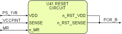
Figure 5: Voltage monitor circuit
Power Rails
Voltages on B2B | B2B J1 Pin | B2B J2 Pin | B2B J3 Pin | Input/ | Note |
|---|---|---|---|---|---|
| PL_VIN | 147, 149, 151, 153, | - | - | Input | supply voltage |
| PS_VIN | - | 154, 156, 158 | - | Input | supply voltage |
| PS_3.3V | - | 160 | - | Input | supply voltage |
| VCCIO12 | 54, 55 | - | - | Input | high range bank I/O voltage |
| VCCIO13 | 112, 113 | - | - | Input | high range bank I/O voltage |
| VCCIO33 | - | - | 115, 120 | Input | high performance bank I/O voltage |
| VCCIO34 | 29, 30 | - | Input | high performance bank I/O voltage | |
| VCCIO35 | 87, 88 | - | Input | high performance bank I/O voltage | |
| VBAT_IN | 146 | - | - | Input | RTC (battery-backed) supply voltage |
| PS_1.8V | - | 130 | - | Output | internal 1.8V voltage level (Process System supply) |
...
Overview
Content Tools