Page History
...
| Scroll Only (inline) |
|---|
Refer to https://shop.trenz-electronic.de/en/Download/?path=Trenz_Electronic/carrier_boards/TEBF0808/REV04 for downloadable version of this manual and additional technical documentation of the product. |
The Trenz Electronic TEBF0808 Carrier Board is a baseboard for the Xilinx Zynq Ultrascale+ MPSoC modules TE0808 and TE0803, which exposes the module's B2B connector pins to accessible connectors and provides a whole range of on-board components to test and evaluate the Zynq Ultrascale+ SoMs and for developing purposes.
Key Features
List key features here, like FPGA type, amount and type of RAM, type of flash, etc.
Additional assembly options are available for cost or performance optimization upon request.
Block Diagram
Put your block diagram here...
Main Components
Put top and bottom pics with labels of the real PCB here...
...
- Mini-ITX form factor
- ATX Power supply connector (Important 12V only Supply Required)
- optional 12V Standard Power Plug
- USB3 with USB3 HUB
- Gigabit Ethernet RJ45
- MicroSD Card (bootable)
- eMMC (bootable)
- PCIe slot - one PCIe lane (16 Lane Connector)
- Displayport Single Lane
- One SATA Connector
- FMC HPC Slot (1.8V max VCCIO)
- Dual SFP+
- One Samtec FireFly (4 GT lanes bidir)
- One Samtec FireFly connector for reverse loopback
- Fan connectors, PC Enclosure, FMC Fan
- Intel front panel connector (PWR/RST/LED)
- Intel HDA Audio connector
- CAN FD Transceiver (10 Pin IDC Connector)
- 20 Pin ARM JTAG Connector (PS JTAG0)
PC Enclosure Rear Panel Accessible I/O
- PCIe accepting 16 Lane PCIe cards (one lane used PS GT)
- FMC HPC
- Dual SFP+
- RJ45 Gigabit Ethernet
- 2x USB3 Host
- Displayport (Single lane)
- microSD
- Two LED's
- CAN FD (using DB9 to IDC10 Cable)
- One PMOD
PC Front Panel I/O
- Reset Button
- Power Button
- Power LED
- HD LED
- Intel HDA Audio
- One USB2 HS Host port
- One USB3 SS Host port
The above I/O interfaces are accessible using standard PC front panel cables.
Additional assembly options are available for cost or performance optimization upon request.
Block Diagram
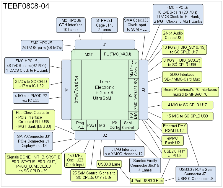
Figure 1: TEBF0808-04 Block Diagram
Main Components
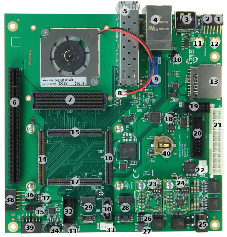
Figure 2: TEBF0808-04 Carrier Board
- PMOD connector, P2
- MicroSD Card socket (on bottom side), J16
- Display Port socket, J13
- USB3.0 A 2x , RJ45 1x (stacked), J7
- SFP+ 2x1 cage, J14
- PCIe x16 connector (one PCIe lane connected), J11
- FMC HPC, J5
- FMC-Fan connector 5V, J19
- USB3.0 connector, J8
- PC-BEEPER 4-pin header, J23
- SMA coaxial connector (SI5338A clock output), J32
- SMA coaxial connector (clock input to MPSoC module), J33
- eMMC Card socket, J27
- Ultra fine 0.50 mm pitch, Razor Beam™ LP Slim Terminal Strip with 160 contacts, J4
- Ultra fine 0.50 mm pitch, Razor Beam™ LP Slim Terminal Strip with 160 contacts, J1
- Ultra fine 0.50 mm pitch, Razor Beam™ LP Slim Terminal Strip with 160 contacts, J3
- Ultra fine 0.50 mm pitch, Razor Beam™ LP Slim Terminal Strip with 160 contacts, J2
- CAN bus 6-pin header, J29
- CAN bus 10-pin connector, J24
- ARM-JTAG 20-pin connector, J30
- ATX power supply connector, J20
- 4-Wire PWM fan connector, J35
- JTAG/UART header ('XMOD FTDI JTAG Adapter'-compatible) for access to MPSoC module, J12
- JTAG/UART header ('XMOD FTDI JTAG Adapter'-compatible) for access to System Controller CPLDs, J28
- Power Jack 2.1mm 12V, J25
- 4x DIP-switch, S5
- Power Button, S1
- Samtec FireFly Connector for reverse loopback, J21/J22
- Samtec FireFly Connector (4 GT lanes bidirectional), J6/J15
- SATA Header, J31
- 4-Wire PWM fan connector, J26
- Programmable on-module PLL I²C interface 10-pin header, J17
- Reset Button, S2
- INTEL HDA 9-pin header, J9
- Intel front panel (PWR/RST/LED) 9-pin header, J10
- Samtec FireFly Connector J6/J15 I²C interface 3-pin header, J34
- 4x DIP-switch, S4
- PMOD connector, P3
- PMOD connector, P1
- Battery Holder CR1220, B1
Initial Delivery State
Storage device name | Content | Notes |
|---|---|---|
|
|
Signals, Interfaces and Pins
...
I/O signals connected to the SoCs I/O bank and B2B connector:
| Bank | Type | B2B Connector | I/O Signal Count | LVDS Pairs Count | Bank Voltage | Notes |
|---|---|---|---|---|---|---|
All MIO banks are powered from on-module DC-DC power rail. All PL I/O Banks have separate VCCO pins in the B2B connectors, valid VCCO should be supplied from the baseboard.
...
| HTML |
|---|
<!-- MGT Lanes should be separately listed, as those are more specifically not just I/O's. --> |
| Bank | Type | Lane Count | B2B Connector | Schematic Names / Connector Pins | FPGA Pin Name | MGT Bank's Reference Clock Inputs |
|---|---|---|---|---|---|---|
| 111 | GTX | 4 | J1 | MGT_RX4_P, MGT_RX4_N, pins J1-23, J1-21 MGT_RX5_P, MGT_RX5_N, pins J1-17, J1-15 MGT_RX6_P, MGT_RX6_N, pins J1-11, J1-9 MGT_RX7_P, MGT_RX7_N, pins J1-3, J1-5 | 1 Reference clock MGT_CLK3 from programmable 1 Reference clock MGT_CLK2 from B2B connector J3 |
JTAG Interface
JTAG access to the ... is provided through B2B connector ....
JTAG Signal | B2B Connector Pin |
|---|---|
| TCK | |
| TDI | |
| TDO | |
| TMS |
System Controller I/O Pins
Special purpose pins are connected to smaller System Controller CPLD and have following default configuration:
| Pin Name | Mode | Function | B2B Connector Pin | Default Configuration |
|---|---|---|---|---|
| PGOOD | Output | Power Good | J1-148 | Active high when all on-module power supplies are working properly. |
| JTAGEN | Input | JTAG Select | J2-131 | Low for normal operation. |
| HTML |
|---|
<!-- For the detailed function of the pins and signals, the internal signal assignment and implemented logic, look to the Wiki reference page SC CPLD of this module or into the bitfile of the SC CPLD. Put in link to the Wiki reference page of the SC CPLD, if available. --> |
...
Quad SPI Flash (U14) is connected to the Zynq PS QSPI0 interface via PS MIO bank 500, pins MIO1 ... MIO6.
| MIO | Signal Name | U14 Pin |
|---|---|---|
| 1 | SPI-CS | C2 |
| 2 | SPI-DQ0/M0 | D3 |
| 3 | SPI-DQ1/M1 | D2 |
| 4 | SPI-DQ2/M2 | C4 |
| 5 | SPI-DQ3/M3 | D4 |
| 6 | SPI-SCK/M4 | B2 |
Gigabit Ethernet
On board Gigabit Ethernet PHY is provided with ...
Ethernet PHY connection
| PHY Pin | PS | PL | B2B | Notes |
|---|---|---|---|---|
USB Interface
USB PHY is provided with ...
| PHY Pin | Pin | B2B Name | Notes |
|---|---|---|---|
The schematics for the USB connector and required components is different depending on the USB usage. USB standard A or B connectors can be used for Host or Device modes. A Mini USB connector can be used for USB Device mode. A USB Micro connector can be used for Device mode, OTG Mode or Host Mode.
...
On-board I2C devices are connected to MIO.. and MIO.. which are configured as I2C... by default. I2C addresses for on-board devices are listed in the table below:
| I2C Device | I2C Address | Notes |
|---|---|---|
Boot Process
By default the ... supports QSPI and SD Card boot modes which is controlled by the MODE input signal from the B2B connector.
MODE Signal State | Boot Mode |
|---|---|
high or open | SD Card |
low or ground | QSPI |
On-board Peripherals
| HTML |
|---|
<!-- Components on the Module, like Flash, PLL, PHY... --> |
...
There is a Silicon Labs I2C programmable quad PLL clock generator Si5338A (U..) ..
| Si5338A (U13) Input | Signal Schematic Name | Note |
|---|---|---|
IN1/IN2 | CLKIN_P, CLKIN_N | Reference clock signal from B2B connector J3, pins J3-74, J3-76 |
IN3 | reference clock signal from oscillator SiTime SiT8008BI (U21) | 25.000000 MHz fixed frequency. |
IN4/IN6 | pins put to GND | LSB (pin 'IN4') of the default I²C-adress 0x70 not activated. |
IN5 | not connected | - |
| Si5338A (U13) Output | Signal Schematic Name | Note |
CLK0 A/B | MGTCLK1_P, MGTCLK1_N | Reference clock signal to MGT bank 112, pins U6/U5 |
| CLK3 A/B | MGTCLK3_P, MGTCLK3_N | Reference clock signal to MGT bank 111, pins AA6/AA5 |
Oscillators
The SoC module has following reference clocking signals provided by external baseboard sources and on-board oscillators:
| Clock Source | Schematic Name | Frequency | Clock Input Destination |
|---|---|---|---|
| SiTime SiT8008BI oscillator, U21 | - | 25.000000 MHz | Quad PLL clock generator U16, pin 3 |
On-board LEDs
| LED | Color | Connected to | Description and Notes |
|---|---|---|---|
Power and Power-On Sequence
...
Xilinx provide a power estimator excel sheets to calculate power consumption. It's also possible to evaluate the power consumption of the developed design with Vivado. See also Trenz Electronic Wiki FAQ.
| Power Input Pin | Typical Current |
|---|---|
| VIN | TBD* |
| 3.3VIN | TBD* |
* TBD - To Be Determined soon with reference design setup.
...
if this circuit is fitted on module, describe it here...
Power Rails
Voltages on B2B-Connectors | B2B | B2B | B2B | Input / Output | Note |
|---|---|---|---|---|---|
Bank Voltages
Bank | Schematic Name | Voltage | Voltage Range |
|---|---|---|---|
| 500 (MIO0) | PS_1.8V | 1.8V | - |
| 501 (MIO1) | PS_1.8V | 1.8V | - |
| 502 (DDR3) | 1.35V | 1.35V | - |
| 12 HR | VCCIO_12 | User | HR: 1.2V to 3.3V |
| 13 HR | VCCIO_13 | User | HR: 1.2V to 3.3V |
| 33 HP | VCCIO_33 | User | HP: 1.2V to 1.8V |
| 34 HP | VCCIO_34 | User | HP: 1.2V to 1.8V |
| 35 HP | VCCIO_35 | User | HP: 1.2V to 1.8V |
Board to Board Connectors
...
Variants Currently In Production
| Module Variant | Zynq SoC | SoC Junction Temperature | Operating Temperature Range |
|---|---|---|---|
| TE0745-02-30-1I | XC7Z030-1FBG676I | –40°C to +100°C | Industrial |
| TE0745-02-35-1C | XC7Z035-1FBG676C | 0°C to +85°C | Commercial |
| TE0745-02-45-1C | XC7Z045-1FBG676C | 0°C to +85°C | Commercial |
| TE0745-02-45-2I | XC7Z045-2FBG676I | –40°C to +100°C | Industrial |
Technical Specifications
Absolute Maximum Ratings
Parameter | Min | Max | Units | Reference Document |
|---|---|---|---|---|
VIN supply voltage | V | - | ||
Storage temperature |
| °C | - |
| Note |
|---|
| Assembly variants for higher storage temperature range are available on request. |
Recommended Operating Conditions
| Parameter | Min | Max | Units | Reference Document |
|---|---|---|---|---|
| VIN supply voltage | ||||
| Operating temperature |
| Note |
|---|
| Please check Xilinx datasheet ... for complete list of absolute maximum and recommended operating ratings. |
...
Hardware Revision History
| Date | Revision | Notes | PCN | Documentation Link |
|---|---|---|---|---|
| - | 01 | Prototypes |
Hardware revision number is printed on the PCB board together with the module model number separated by the dash.
...
| HTML |
|---|
<!-- Generate new entry: 1.add new row below first 2.Copy "Page Information Macro(date)" Macro-Preview, MetaData Version number, Autor Name and description to the empty row. Important Revision number must be the same as the Wiki document revision number 3.Update Metadate = "Page Information Macro (current-version)" Preview+1 and add Autor and change description. --> |
Date | Revision | Contributors | Description | ||||||||
|---|---|---|---|---|---|---|---|---|---|---|---|
| John Hartfiel | -removed weight section update template version | |||||||||
2017-06-08 | v.20 | John Hartfiel | add revision number and update document change history | ||||||||
2017-05-30 | v.1 | Jan Kumann | Initial document. | ||||||||
all | Jan Kumann, John Hartfiel |
Disclaimer
| Include Page | ||||
|---|---|---|---|---|
|
...
Overview
Content Tools