Page History
...
| HTML |
|---|
<!-- Template Revision 1.6465 (HTML comments will be not displayed in the document, no need to remove them. For Template/Skeleton changes, increase Template Revision number. So we can check faster, if the TRM style is up to date). --> |
...
| HTML |
|---|
<!-- Download Link: Go to Base Folder of the Module or Carrier, for example : https://shop.trenz-electronic.de/en/Download/?path=Trenz_Electronic/TE0712 Use english URL "../en/.. --> |
| Scroll Ignore |
|---|
Download PDF version of this document. |
| Scroll pdf ignore | |
|---|---|
Table of Contents
|
Overview
| HTML |
|---|
<!-- Wiki Link: Go to Base Folder of the Module or Carrier, for example : https://wiki.trenz-electronic.de/display/PD/TE0706TE0712 --> |
| Scroll Only (inline) |
|---|
Refer to https://wiki.trenz-electronic.de/display/PD/TEBA0841+TRMTEM0001 for the current online version of this manual and other available documentation. |
The Trenz Electronic TEBA0841 is a Carrier Board for testing, evaluation and development purposes, especially for the Multi-gigabit transceiver units of the TE0841 and TE0741 modules. Although this base-board is dedicated to the modules TE0841 and TE0741, it is also compatible with other Trenz Electronic 4 x 5 cm SoMs.
See page "4 x 5 cm carriers" to get information about the SoMs supported by the TEBA0841 base-board.
Key Features
- SFP+ connector (Enhanced small form-factor pluggable), supports data transmission rates up to 10 Gbit/s
- Micro USB2.0 Type B Connector (J10)
- Trenz 4x5 module Socket (3 x Samtec LSHM series connectors)
- 4 x 5 SoM programmable by XMOD JTAG/UART header (JX1)
- 2 x user LEDs routed to I/O-pins of the SoM
- Soldering-pads J17 and J20 for optional pin headers for access to SoM's I/O-bank-pins, usable as LVDS-pairs
- Soldering-pads J3 and J4 for optional pin headers for access to further interfaces and I/O's of the SoM
Additional assembly options are available for cost or performance optimization upon request.
Block Diagram
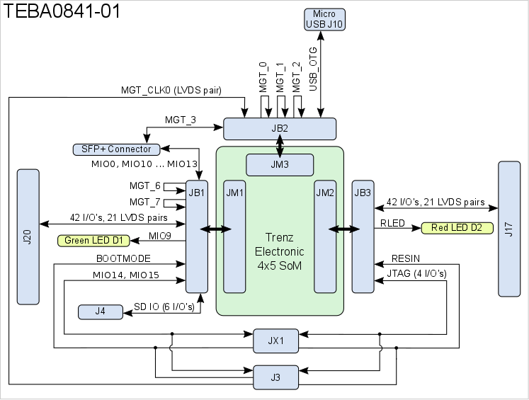
Figure 1: TEBA0841-01 Block Diagram.
Main Components
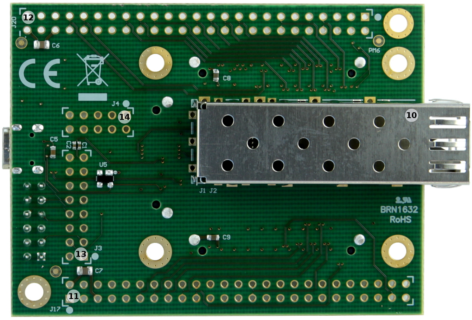
Figure 2: TE0706-02 Carrier Board.
- Samtec Razor Beam™ LSHM-150 B2B connector, JB1
- Samtec Razor Beam™ LSHM-150 B2B connector, JB3
- Samtec Razor Beam™ LSHM-130 B2B connector, JB2
- 6-pin header J26, for selecting PL I/O-bank voltage
- 6-pin header J27, for selecting PL I/O-bank voltage
- Micro USB2.0 Type B Connector J12 (Device or OTG mode)
- JTAG/UART header, JX1 ('XMOD FTDI JTAG Adapter'-compatible pin-assignment)
- User LED D1 (green)
- User LED D2 (red)
- SFP+ Connector, J1
- 50-pin header soldering-pads J17, for access to PL I/O-bank pins (LVDS-pairs possible)
- 50-pin header soldering-pads J20, for access to PL I/O-bank pins (LVDS-pairs possible)
- 16-pin header soldering-pads J3, JTAG/UART header ('XMOD FTDI JTAG Adapter'-compatible pin-assignment)
- 10-pin header soldering-pads J4, for access to SoM's SDIO-port, if available
Initial Delivery State
Board is shipped in following configuration:
- VCCIO voltage selection jumpers are all set to 1.8 V.
- Pin headers (not soldered to the board, but included in the package as separate component)
Different delivery configurations are available upon request.
Signals, Interfaces and Pins
| HTML |
|---|
<!--
Connections and Interfaces or B2B Pin's which are accessible by User
--> |
B2B Connector
With the TEBA0841 Carrier Board's Board-to-Board Connectors (B2B) the MIO- and PL I/O-bank's pins and further interfaces of the mounted SoM can be accessed. A large quantity of these I/O's are also usable as differential pairs. The connectors provide also VCCIO voltages to operate the I/O's properly.
Following table gives a summary of the available I/O's, interfaces and differential pairs of the B2B connectors JB1, JB2 and JB3:
...
Table 1: General overview of PL I/O signals and SoM's interfaces connected to the B2B connectors.
On-board Pin Header
The TEBA0841 Carrier Board has 4 footprints as soldering pads to mount 2.54mm grid size pin headers to get access the PL I/O-bank's pins and further interfaces of the mounted SoM. With these pin headers, SoM's PL-I/O's are available to the user, a large quantity of these I/O's are also usable as differential pairs.
Following table gives a summary of the pin-assignment, available interfaces and functional I/O's of the pin headers:
...
User I/O
...
Table 2: General overview of PL I/O signals, SoM's interfaces and control signals connected to the on-board connectors.
SFP+ Connector
On the TEBA0841 carrier board is a SFP+ connector J1 (board-rev. 01: Molex 74441-0001). The connector is embedded into a SFP cage J2 (board-rev. 01: Molex 74737-0009).
The differential RX/TX data lanes are connected to B2B connector JB2, the control-lines are connected to B2B connector JB1 and are assigned to MIO-bank pins of the mounted SoM.
The pin-assignment of the SFP connector is in detail as fellows:
...
Table 1: SFP+ connector pin-assignment.
1) Important: For proper operation, a wire patch to GND is done at recently delivered boards. Connect to GND, if not done. See PCB drawing below:
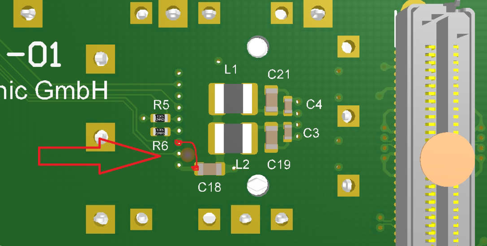
Figure 3: PCB wire patch for SFP+ connector.
Looped-backed MGT-Lanes on B2B Connector JB1 and JB2
The TEBA0841 carrier board is mainly designed for the 4 x 5 SoMs TE0841 and TE0741. This SoMs have GTX-Transceiver units on their FPGA-modules with up to 8 available MGT-lanes. To test this MGT-lanes, 5 RX/TX differential pairs are bridged on-board, hence the transmitted data on this MGT-lanes flows back to their sources in a loop-back circuit without intentional processing or modification.
The MGT lane pins are bridged on-board as fellows, if 4 x 5 SoM TE0741 is mounted on carrier board:
...
JB2-8 (MGT_TX0_N)
JB2-10 (MGT_TX0_P)
...
JB2-7 (MGT_RX0_N)
JB2-9 (MGT_RX0_P)
...
JB2-7 to JB2-8
JB2-9 to JB2-10
...
JB2-14 (MGT_TX1_N)
JB2-16 (MGT_TX1_P)
...
JB2-13 (MGT_RX1_N)
JB2-15 (MGT_RX1_P)
...
JB2-13 to JB2-14
JB2-15 to JB2-16
...
JB2-20 (MGT_TX2_N)
JB2-22 (MGT_TX2_P)
...
JB2-19 (MGT_RX2_N)
JB2-21 (MGT_RX2_P)
...
JB2-19 to JB2-20
JB2-21 to JB2-22
...
JB1-3 (MGT_TX7_P)
JB1-5 (MGT_TX7_N)
...
JB1-9 (MGT_RX7_P)
JB1-11 (MGT_RX7_N)
...
JB1-3 to JB1-9
JB1-5 to JB1-11
...
JB1-15 (MGT_TX6_P)
JB1-17 (MGT_TX6_N)
...
JB1-21 (MGT_RX6_P)
JB1-23 (MGT_RX6_N)
...
JB1-15 to JB1-21
JB1-17 to JB1-23
TEM0001 is a low cost small-sized FPGA module integrating a Microsemi SmartFusion2 FPGA SoC and 8 MByte Flash memory for configuration and operation.
Key Features
Microsemi SmartFusion2 SoC FPGA
- 8 MByte SDRAM
8 MByte QSPI Flash memory
- 25 MHz system clock and 32.768 KHz auxiliary clock
- JTAG and UART over Micro USB connector
- 1x 3-pin header for Live Probes
- 1x PMOD header providing 8 I/O
2x 14-pin headers (2,54 mm pitch) providing 23 I/O
9 user LEDs
- 1 user push button
- 3.3V single power supply with on-board voltage regulators
- Size 61.5 x 25 mm
Additional assembly options are available for cost or performance optimization upon request.
Block Diagram
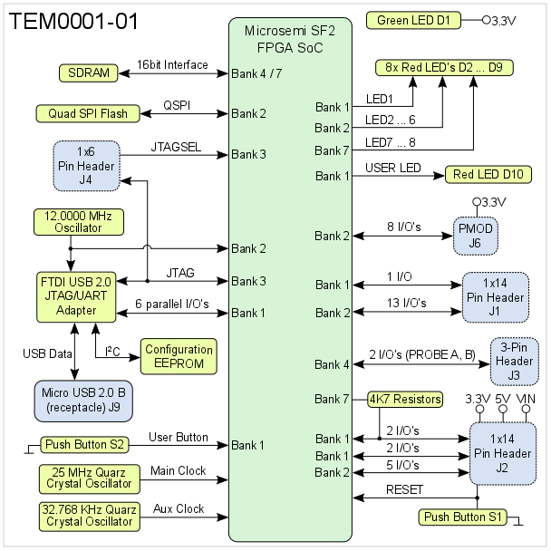
Figure 1: TEM0001-01 block diagram
Main Components
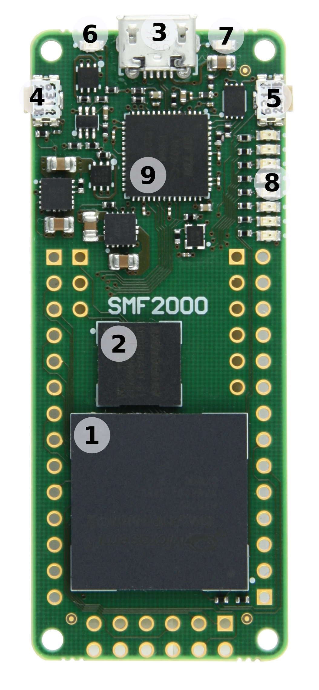
Figure 2: TEM0001-01 FPGA module
- Microsemi SmartFusion2 FPGA SoC, U5
- 8 Mbyte SDRAM 166MHz, U2
- Micro USB2 B socket (receptacle), J9
- Switch button (reset), S1
- Switch button (user), S2
- Red LED (user), D10
- Green LED (indicating supply voltage), D1
- 8x red LEDs (user), D2 - D9
- FTDI USB2 to JTAG/UART interface, U3
- 8 Mbyte QSPI Flash memory, U1
- 32.768 KHz auxiliary crystal, Y1
- 25 MHz main crystal, Y2
- 1x14 pin header (2.54mm pitch), J2
- 1x6 pin header (2.54mm pitch), J4
- 3-pin header (2.54mm pitch), J3
- 1x14 pin header (2.54mm pitch), J1
- 2x6 Pmod connector, J6
Initial Delivery State
Storage device name | Content | Notes |
|---|---|---|
SPI Flash OTP area | empty | - |
| SPI Flash | empty | - |
| FTDI EEPROM, U9 | Programmed | FlashPro identification, should not be changed by customer |
Table 1: Initial delivery state of programmable devices on the module
Boot Process
There is are no bootmode selection Microchip SmartFusion2 SoC boots always from internal configuration flash, optionally software code for the Cortex-M or soft CPU can be placed to eNVM.
Signals, Interfaces and Pins
I/Os on Pin Headers and Connectors
I/O signals of the FPGA SoC's I/O banks connected to the board's pin headers and connectors:
| Bank | Connector Designator | I/O Signal Count | Bank Voltage | Notes |
|---|---|---|---|---|
| 1 | J1 | 1 I/O's | 3.3V | - |
| 1 | J2 | 4 I/O's | 3.3V | 2 I/O's of bank 1 can be pulled-up to 3.3V (4K7 resistors) with 2 I/O's of Bank 7 or pins can be shared. |
| 2 | J1 | 13 I/O's | 3.3V | - |
| 2 | J2 | 5 I/O's | 3.3V | - |
| 2 | J6 | 8 /O's | 3.3V | Pmod Connector. |
| 3 | J4 | 5 I/O's | 3.3V | JTAG interface. |
| 4 | J3 | 2 I/O's | 3.3V | I/O's (PROBE A, B) are dedicated to live probes. |
| 7 | J2 | 2 I/O's | 3.3V | Those 2 I/O's are dedicated to pull-up 2 I/O's of bank 1 or pins can be shared. |
Table 2: General overview of single ended I/O signals connected to pin headers and connectors
FPGA I/O banks
| Bank | VCCIO | I/O's Count | Available on Connectors | Notes |
|---|---|---|---|---|
| 1 | 3.3V | 14 | 5 | 6 I/O's connected to FTDI chip, 1 I/O used for user button S2, 2 I/O's connected to red user LEDs D2 and D10. |
| 2 | 3.3V | 37 | 26 | 6 I/O's user for QSPI Flash, 5 I/O's connected to red user LEDs D3 ... D7. |
| 3 | 3.3V | 5 | 5 | Bank 3 is dedicated to JTAG interface. |
| 4 | 3.3V | 24 | 2 | 2 I/O's are dedicated to live probes, all other I/O's are used as memory interface. |
| 7 | 3.3V | 22 | 2 | 2 I/O's available on header J2, 2 I/O's connected to red user LEDs D8 and D9, all other I/O's are used as memory interface. |
Table 3: General overview of FPGA I/O banks
JTAG Interface
JTAG access to the FPGA SoC device U5 is provided through Micro USB2 B connector J9. The JTAG interface is implemented with FTDI FT2232H USB2 to JTAG/UART bridge IC U3.
Optionally 1x6 male pin header J4 can be fitted on board for access to the JTAG interface on board. The pin assignment of header J4 is shown on table below:
| JTAG Signal | Pin on Header J4 | Note |
|---|---|---|
| TCK | 3 | - |
| TDI | 5 | - |
| TDO | 4 | - |
| TMS | 6 | - |
| JTAGSEL | 2 | can be left open for normal operation |
Table 4: optional JTAG header
QSPI Interface
The QSPI interface of the FPGA device is routed to and used by the on-module QSPI flash IC U1:
| SD IO Signal Schematic Name | FPGA I/O | Flash IC U1 Pin | Note |
|---|---|---|---|
| F_CS | Bank 2, pin K15 | 1 | QSPI chip select |
| F_CLK | Bank 2, pin P18 | 6 | QSPI clock |
| F_DI | Bank 2, pin P19 | 5 | QSPI data |
| F_DO | Bank 2, pin K16 | 2 | QSPI data |
| F_D2 | Bank 2, pin J18 | 3 | QSPI data |
| F_D3 | Bank 2, pin N19 | 7 | QSPI data |
Table 5: QSPI interface signals
Note: On-board SPI Flash is connected to regular FPGA I/O pins, access to it is only possible when using custom SPI flash IP core or via MSS subsystem SPI when it is connected via fabric to those pins. There is no automatic boot from this flash.
On-board Peripherals
Quad SPI Flash Memory
On-module QSPI flash memory (U7) is provided by Winbond Serial Flash Memory W74M64FV with 64 MBit (8 MByte) storage capacity.
SDRAM
The TEM0001 FPGA module is equipped with a Winbond W9864G6JT 64 MBit (8 MByte) SDRAM chip U2.
FTDI FT2232H IC
FTDI FT2232H Channel A works as JTAG interface compatible to Libero tools. Channel B is connected to FPGA pins with direct access to MSS UART peripheral.
The configuration of FTDI FT2232H is pre-programmed to the EEPROM U9 to make it work as FlashPro5 interface for Libero tools.
System Clock Oscillator
The FPGA SoC module has following reference clocking signals provided by on-board oscillators:
| Clock Source | Schematic Name | Frequency | Clock Input Destination |
|---|---|---|---|
| MEMS Oscillator, U7 | CLK12M | 12.0000 MHz | FTDI FT2232 U3, pin 3; FPGA SoC bank 2, pin N16 |
Crystal Oscillator, Y1 | - | 32.768 KHz | FPGA SoC U5 auxiliary clock, pins W17/Y17 |
| Quartz Crystal Oscillator, Y2 | - | 25.000 MHz | FPGA SoC U5 main clock, pins W18/Y18 |
Table 6: Clock sources overview
On-board LEDs
There are 10 LEDs fitted on the FPGA module board. The LEDs are user configurable to indicate for example any system status.
| LED | Color | Signal Schematic Name | FPGA | Notes |
|---|---|---|---|---|
| D1 | Green | - | - | Indicating 3.3V board supply voltage |
| D2 | Red | LED1 | E18 | user |
| D3 | Red | LED2 | R17 | user |
| D4 | Red | LED3 | R18 | user |
| D5 | Red | LED4 | T18 | user |
| D6 | Red | LED5 | U18 | user |
| D7 | Red | LED6 | R16 | user |
| D8 | Red | LED7 | E1 | user |
| D9 | Red | LED8 | D2 | user |
| D10 | Red | USER_LED | G17 | user |
Table 7: LEDs of the module
Push Buttons
The TEM0001 FPGA module is equipped with two push buttons S1 and S2:
| Button | Signal Schematic Name | FPGA | Notes |
|---|---|---|---|
| S1 | USER_BTN | B19 | user configurable |
| S2 | RESET | U17 | system reset (reconfiguration) |
Table 8: Push buttons of the module
Connectors
All connectors are are for 100mil headers, all connector locations are in 100mil (2.54mm) grid. The module's PCB provides footprints to mount and solder optional pin headers, if those are not factory-fitted on module.
Power and Power-On Sequence
To power-up a module, power supply with minimum current capability of 1A is recommended.
Power Supply
The FPGA module can be power-supplied through Micro USB2 connector J9 with supply voltage 'USB-VBUS' or alternative through pin header J2 with supply voltage 'VIN'.
The TEM0001 module needs one single power supply of 5.0V nominal.
There are following dependencies how the initial voltage of the extern power supply is distributed to the on-board DCDC converters:
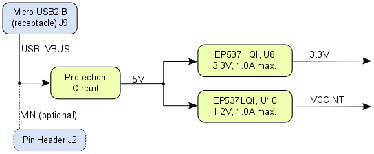
Figure 3: Power Distribution Diagram
Power Consumption
| FPGA | Design | Typical Power, 25C ambient |
|---|---|---|
| Mircosemi SmartFusion2 FPGA SoC M2S010-VFG400 | Not configured | TBD* |
Table 9: Module power consumption
*TBD - To Be Determined.
Actual power consumption depends on the FPGA design and ambient temperature.
Power-On Sequence
There is no specific or special power-on sequence, just one single power source is needed.
Table 2: Looped-backed MGT-lanes for mounted 4 x 5 SoM TE0741.
| Note |
|---|
| Note: The mounted TE 4 x 5 SoMs have different schematic net-names of the differential signaling pairs of the MGT-lanes. See Schematic of the particular SoM. |
JTAG Interface
JTAG access to the mounted SoM is provided through B2B connector JB2 and is also routed to the XMOD header JX1 and pin header J3. With the TE0790 XMOD USB2.0 to JTAG adapter, the device of the mounted SoM can be programed via USB2.0 interface.
...
JTAG Signal
...
B2B Connector Pin
...
Table 3: JTAG interface signals.
UART Interface
UART interface is available on B2B connector JB1 and is usually established by MIO-pins of the PS-bank of the mounted SoM's Zynq device. With the TE0790 XMOD USB2.0 adapter, the UART signals can be converted to USB2.0 interface signals:
...
Table 4: UART interface signals.
SD IO Interface
The SD IO interface of the mounted SoM is routed to the pin header J4. Due to the different operation voltage levels of the MicroSD Card socket (3.3V) and the and the SoM's Zynq device MIO-bank (1.8V), a VDD/VCCIO translation is necessary which can be provided for example by Texas Instruments TXS02612 SDIO port expander IC. Both voltage levels are available on pin header J4:
...
Table 6: SD IO interface signals.
USB2.0 Interface
TEBA0841 board has one physical Micro USB2.0 type B socket J10, the differential data signals of the USB2.0 socket are routed to the B2B connector JB2, where they can be accessed by the corresponding USB2.0 PHY transceiver of the mounted SoM.
With Micro USB2.0 type B socket, the USB2.0 interface can also be used in Device or OTG mode.
Following table gives an overview of the USB2.0 interface signals:
...
JB2-48
...
Table 7: USB2.0 interface signals and connections.
XMOD FTDI JTAG-Adapter Header
The JTAG interface of the mounted SoM can be accessed via XMOD header JX1 and pin header J3, which has a 'XMOD FTDI JTAG Adapter'-compatible pin-assignment, but also two additional pins (15,16) as differential pairs to supply the mounted SoM with an external MGT reference clock signal.
So in use with the XMOD-FT2232H adapter-board TE0790 the mounted SoM can be programmed via USB2.0 interface. The TE0790 board provides also an UART interface to the SoM's Zynq device which can be accessed by the USB2.0 interface of the adapter-board while the signals between these serial interfaces will be converted.
Following table describes the signals and interfaces of the XMOD header JX1 and pin header J3:
...
When using XMOD FTDI JTAG Adapter TE0790, the adapter-board's VCC and VCCIO will be sourced by the on-boards 3.3V supply voltage. Set the DIP-switch with the setting:
...
| Note |
|---|
Use Xilinx compatible TE0790 adapter board (designation TE-0790-xx with out 'L') to program the Xilinx Zynq devices. The TE0790 adapter board's CPLD have to be configured with the Standard variant of the firmware. Refer to the TE0790 Resources Site for further information and firmware download. |
On-board Peripherals
| HTML |
|---|
<!--
Components on the Module, like Flash, PLL, PHY...
--> |
On-board LEDs
The on-board LEDs are available to the user and can be used to indicate system status and activities:
...
Figure 3: On-board LEDs
VCCIO Selection Jumper
On the TEBA0841 carrier board different VCCIO configurations can be selected by the jumper J26 and J27.
TE 4 x 5 Modules have a standard assignment of PL-bank I/O voltages on their B2B connectors, which will be fed with I/O voltage from base-board.
...
Base-board PL-bank I/O Voltages
...
Table 5: Base-board PL-bank I/O voltages VCCIOA and VCCIOD
| Note |
|---|
Note: The corresponding PL-bank I/O voltages of the 4 x 5 SoM to the selectable base-board voltages VCCIOA and VCCIOD are depending on the mounted 4 x 5 SoM and varying in order of the used model. Refer to the SoM's schematic for information about the specific pin assignments on module's B2B-connectors regarding the PL-bank I/O voltages and to the 4 x 5 Module integration Guide for VCCIO voltage options. |
Following table describes how to configure the base-board supply-voltages by jumpers:
...
Base-board PL-bank I/O Voltages
vs Voltage Levels
...
Table 6: Configuration of base-board supply-voltages via jumpers. Jumper-Notification: 'Jx: 1-2' means pins 1 and 2 are connected, 'Jx: 3-4' means pins 3 and 4 are connected, and so on.
| Note |
|---|
Take care of the VCCO voltage ranges of the particular PL IO-banks (HR, HP) of the mounted SoM, otherwise damages may occur to the FPGA. Therefore, refer to the TRM of the mounted SoM to get the specific information of the voltage ranges. It is recommended to set and measure the PL IO-bank supply-voltages before mounting of TE 4 x 5 module to avoid failures and damages to the functionality of the mounted SoM. |
Power and Power-On Sequence
| HTML |
|---|
<!--
If power sequencing and distribution is not so much, you can join both sub sections together
--> |
Power Consumption
The maximum power consumption of the Carrier Board depends mainly on the mounted SoM's FPGA design running on the Zynq device.
Xilinx provide a power estimator excel sheets to calculate power consumption. It's also possible to evaluate the power consumption of the developed design with Vivado. See also Trenz Electronic Wiki FAQ.
...
Table 14: Typical power consumption.
* TBD - To Be Determined soon with reference design setup.
Power supply with minimum current capability of 3A for system startup is recommended.
| Warning |
|---|
| To avoid any damage to the module, check for stabilized on-board voltages and VCCIO's before put voltages on PL I/O-banks and interfaces. All I/Os should be tri-stated during power-on sequence. |
Power Supply
Power supply with minimum current capability of 3A at 3.3V for system startup is recommended.
The on-board voltages of the carrier board will be powered up with an external power-supply with nominal voltage of 3.3V.
The external power-supply can be connected to the board by the following pins:
...
JX1-5, JX1-6,
...
Table 4: Connector pins capable for external 3.3V power supply
Power Distribution Dependencies
The PL-bank I/O voltages 1.8V, 2.5V and 3.3V will be available after the mounted SoM's 3.3V voltage level has reached stable state on B2B-connector pins JM2-10 and JM2-12, meaning that all on-module voltages have become stable and module is properly powered up.
Following diagram shows the distribution of the external input voltage of nominal 3.3V to the components:
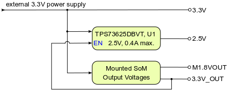
Figure 5: Board power distribution diagram.
Power Rails
...
3.3V
...
2, 4, 6, 14, 16
...
3.3V_OUT
...
9, 11
...
Table 15: Power pin description of B2B module connector.
...
3.3V
...
5, 48
...
3.3V
...
5, 48
...
Table 16: Power Pin description of on-board connector.
...
VCCIOD
...
Table 17: Power Pin description of VCCIO selection jumper pin header.
...
Table 19: Power pin description of peripheral connector.
...
Table 20: Power pin description of XMOD/JTAG Connector.
Board to Board Connectors
Include Page
Technical Specifications
Absolute Maximum Ratings
Parameter | Min | Max | Units |
|---|
| Reference document |
|---|
Vin supply voltage
3.135
V
VIN supply voltage (5.0V nominal) | -0.3 | 6.0 | V | EP53A7HQI / EP53A7LQI datasheet |
| I/O Input voltage for FPGA I/O bank | -0.3 | 3.63 | V | Microsemi datasheet DS0128 |
Storage Temperature | - |
40 |
+90 | °C |
| LED R6C-AL1M2VY/3T datasheet |
Table 2210: Board absolute Absolute maximum ratings.
Recommended Operating Conditions
...
Recommended Operating Conditions
| Parameter | Min | Max | Units | Reference document |
|---|---|---|---|---|
| VIN supply voltage (5.0V nominal) | 4.75 | 5.25 | V | same as USB-VBUS specification |
| I/O Input voltage for FPGA I/O bank | 0 | 3.45 | V | Microsemi datasheet DS0128 |
| Operating temperature range | 0 | +70 | °C | Winbond datasheet W9864G6GT |
Table 11: Recommended operating conditions
| Note |
|---|
| Please check Microsemi datasheet DS0128 for complete list of absolute maximum and recommended operating ratings for the FPGA device. |
Physical Dimensions
Please note that two different units are used on the figures below, SI system millimeters (mm) and imperial system thousandths of an inch(mil). This is because of the 100mil pin headers used, see also explanation below. To convert mils to millimeters and vice versa use formula 100mil's = 2,54mm.
Board size: PCB 25mm × 61,5mm
Table 23: Module recommended operating conditions.
Operating Temperature Ranges
Industrial grade: -40°C to +85°C.
The TEBA0841 Carrier Board itself is capable to be operated at industrial grade temperature range.
Please check the operating temperature range of the mounted SoM, which determine the relevant operating temperature range of the overall system.
Physical Dimensions
Board size: PCB 56.47 mm × 75 mm. Notice that some parts the are hanging slightly over the edge of the PCB like the mini USB-jacks and the SFP+ the Micro USB2 B connector, which determine the total physical dimensions of the carrier board. Please download the assembly diagram for exact numbers.
Mating height of the module with standard connectors: 8mm
PCB thickness: ca. 1.65mm
Highest part on the PCB is the SFP+ without fitted headers and connectors is the Micro USB2 B connector, which has an approximately 11.hight of 3 mm overall hight. Please download the step model for exact numbers.
The dimensions are given in mm and mil (milli inch).
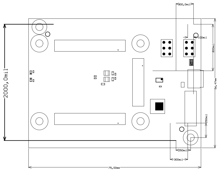
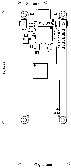
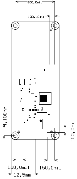
Figure 4: Module Figure 6: Board physical dimensions drawing.
Revision History
Hardware Revision History
| Date | Revision | Notes | PCN | Documentation Link |
|---|---|---|---|---|
| - | 01 |
| - | TEBA0841-01 |
Table 24: Module hardware revision history.
...
Table 12: Module hardware revision history
Hardware revision number is printed on the PCB board together with the module model number separated by the dash.
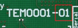
Figure 5: Module hardware revision number
Document Change History
| Date | Revision | Contributors | Description | ||||||||||||||||||||||
|---|---|---|---|---|---|---|---|---|---|---|---|---|---|---|---|---|---|---|---|---|---|---|---|---|---|
|
|
|
| ||||||||||||||||||||||
| v.33 | Antti Lukats |
| |||||||||||||||||||||||
2018-04-17 | v.31 | Ali Naseri |
|
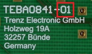
Figure 7: Board hardware revision number.
Document Change History
| HTML |
|---|
<!--
Generate new entry:
1.add new row below first
2.Copy "Page Information Macro(date)" Macro-Preview, Metadata Version number, Author Name and description to the empty row. Important Revision number must be the same as the Wiki document revision number
3.Update Metadata = "Page Information Macro (current-version)" Preview+1 and add Author and change description.
--> |
...
Date
...
Revision
...
Contributors
...
Description
...
- First TRM release
Table 25: Document change history.Table 13: Document change history
Disclaimer
| Include Page | ||||
|---|---|---|---|---|
|
Overview
Content Tools