Page History
...
Table 2: Count, type and voltage range of SoC's PL and PS I/O banks pins available through B2B connectors.
All MIO banks are powered from on-module DC-DC power rail. All PL I/O Banks have separate VCCO pins in the B2B connectors, valid VCCO should be supplied from the baseboard.
...
Below are listed MGT banks reference clock sources.
| Clock signal | Bank | Source | FPGA Pin | Notes |
|---|---|---|---|---|
| MGT_CLK0_P | 112 | B2B, J3-75 | MGTREFCLK0P_112, R6 | Supplied by the carrier board. |
| MGT_CLK0_N | 112 | B2B, J3-77 | MGTREFCLK0N_112, R5 | Supplied by the carrier board. |
| MGT_CLK1_P | 112 | U16, CLK0A | MGTREFCLK1P_112, U6 | On-module Si5338A. |
| MGT_CLK1_N | 112 | U16, CLK0B | MGTREFCLK1N_112, U5 | On-module Si5338A. |
| MGT_CLK2_P | 111 | B2B, J3-81 | MGTREFCLK0P_111, W6 | Supplied by the carrier board. |
| MGT_CLK2_N | 111 | B2B, J3-83 | MGTREFCLK0N_111, W5 | Supplied by the carrier board. |
| MGT_CLK3_P | 111 | U16, CLK3A | MGTREFCLK1P_111, AA6 | On-module Si5338A. |
| MGT_CLK3_N | 111 | U16, CLK3B | MGTREFCLK1N_111, AA5 | On-module Si5338A. |
Table 4: MGT reference clock sources.
...
The I2C interface on B2B connector J2 has PS_3.3V as reference voltage and is connected to the Zynq SoC via voltage level translating (3.3V ↔ 1.8V) I2C bus repeater (U17).:
| B2B pin | Signal Schematic Name | Notes |
|---|---|---|
| J2-119 | I2C_33_SCL | 3.3V reference voltage |
| J2-121 | I2C_33_SDA | 3.3V reference voltage |
Table 10: Pin assignment of the B2B I2C interface.
...
| Boot Mode | MIO5 (BOOTMODE_1), SC CPLD | MIO4 (BOOTMODE), J2-133 | MIO3 | Note |
|---|---|---|---|---|
JTAG | 0 | 0 | 0 | - |
| NOR | 0 | 0 | 1 | MIO3 pin is shared with QSPI Flash Memory (QSPI-DQ1). |
| NAND | 0 | 1 | 0 | - |
| QSPI Flash Memory | 1 | 0 | 0 | standard mode in current configuration. |
| SD-Card | 1 | 1 | 0 | SD-Card on base board necessary. |
Table 1113: Selectable boot modes.
In delivery state of the SoM the boot mode depends on the configured SC-CPLD firmware. The current mode is set to boot from the QSPI Flash Memory.
...
Once running, the frequency and other parameters can be changed by programming the device using the I2C-bus connected between the Zynq module (master) and reference clock signal generator (slave).
| Si5338A |
|---|
| Pin | Signal |
|---|
| Name / Description | Connected To | Direction | Note |
|---|---|---|---|
IN1 |
CLKIN_P | B2B, J3-76 | Input | Reference input clock from base board. | |
| IN2 | CLKIN_N |
| B2B |
| , |
| J3-74 |
(base board decoupling capacitors and termination resistor necessary).
| Input | |
IN3 |
Reference input clock. | Oscillator U21, pin 3 | Input | 25.000000 MHz |
| oscillator, Si8008BI. |
IN4 |
IN5
not connected
CLK0 A/B
MGTCLK1_P, MGTCLK1_N
Reference clock signal to MGT bank 112, pins U6/U5
(100 nF decoupling capacitors).
CLK1 A/B
Clock signal routed to B2B connector, pins J3-80, J3-82.
CLK2 A/B
Clock signal routed to B2B connector, pins J3-86, J3-88.
MGTCLK3_P, MGTCLK3_N
Reference clock signal to MGT bank 111, pins AA6/AA5
(100 nF decoupling capacitors).
Table 12: Pin description of PLL clock generator Si5338A
| - | GND | Input | ||||
| Si5338A Pin | Signal Name / Description | Connected To | Direction | Note | ||
|---|---|---|---|---|---|---|
IN1 | CLKIN_P | Not connected. | Input | Not used. | ||
| IN2 | - | GND | Input | Not used. | ||
IN3 | Reference input clock. | U3, pin 3 | Input | 25.000000 MHz oscillator, Si8208AI. | ||
IN4 | - | GND | Input | I2C slave device address LSB (0x70 default address). | ||
IN5 | - | Not connected. | Input | Not used. | ||
| IN6 | - | GND | Input | Not used. | ||
CLK0A | MGT_CLK1_P | Zynq Soc U1, R23pin U6 | OutputFPGA | MGT bank | 45112 reference clock. | |
| CLK0B | MGT_CLK1_N | Zynq Soc U1, P23pin U5 | OutputFPGA bank 45. | |||
| CLK1A | MGT_CLK1_NP | U1B2B, V5J3-80 | OutputFPGA MGT bank 225 reference clock | Reference clock output to base board. | ||
| CLK1B | MGT_CLK1_PN | U1B2B, V6J3-82 | OutputFPGA MGT bank 225 reference clock. | |||
| CLK2A | MGTCLK2_CLK3_NP | U1B2B, AB5J3-86 | OutputFPGA MGT bank 224 reference clock | Reference clock output to base board. | ||
| CLK2B | MGT_CLK3CLK2_P | U1B2B, AB6J3-88 | Output | |||
| FPGA MGT bank 224 reference clock. | CLK3A | CLK0MGT_CLK3_P | Zynq Soc U1, pin T24AA6 | OutputFPGA | MGT bank | 45111 reference clock. |
| CLK3B | CLK0MGT_CLK3_N | Zynq Soc U1, pin T25AA6 | OutputFPGA bank 45 |
Table 14: Programmable quad PLL clock generator inputs and outputs.
Oscillators
The SoC module has following reference clocking signals provided by external baseboard sources and on-board oscillators:
| Clock Source | Schematic Name | Frequency | Clock Input Destination |
|---|---|---|---|
| SiTime SiT8008BI oscillator, U21 | - | 25.000000 MHz | Quad PLL clock generator U16, pin 3 |
SiTime SiT8008BI oscillator, U12 | PS_CLK | 33.333333 MHz | Bank 500 (MIO0 bank), pin B24 |
| SiTime SiT8008BI oscillator, U33 | OTG-RCLK | 52.000000 MHz | USB 2.0 transceiver PHY U32, pin 26 |
| SiTime SiT8008BI oscillator, U9 | ETH_CLKIN | 25.000000 MHz | Gigabit Ethernet PHY U7, pin 34 |
Table 1315: Clock sources overview.
On-board LEDs
| LED | Color | Connected to | Description and Notes |
|---|---|---|---|
D1 | Green | System Controller CPLD, bank 3, pin 5 | System main status LED, blinking indicates system activity |
D2 | Red | Zynq chip (U1), bank 0 (config bank), 'DONE' (pin W9) | Reflects inverted DONE signal. ON when FPGA is not configured, OFF as soon as PL is configured. This LED remains OFF if System Controller CPLD can not power up the PL supply voltage. |
Table 1416: LEDs of the module.
Power and Power-On Sequence
...
| Power Input Pin | Typical Current |
|---|---|
| PL_VIN | TBD* |
| PS_VIN | TBD* |
| PS_3.3V | TBD* |
Table 1517: Maximum current of Typical power suppliesconsumption. *to be determined soon with reference design setup.
Power supply with minimum current capability of 3A for system startup is recommended.
...
| Warning |
|---|
| To avoid any damage to the SoC module, check for stabilized on-board voltages in steady state before powering up the SoCfor stabilized on-board voltages should be carried out(i.e. power good and enable signals) before powering up any SoC's I/O bank voltages VCCO_x. All I/O's Os should be tri-stated during power-on sequence. |
...
Figure 5: Voltage monitor circuit.
Power Rails
Voltages on B2B | B2B J1 Pin | B2B J2 Pin | B2B J3 Pin | Input/ | Note |
|---|---|---|---|---|---|
| PL_VIN | 147, 149, 151, 153, | - | - | Input | module supply voltage |
| PS_VIN | - | 154, 156, 158 | - | Input | module supply voltage |
| PS_3.3V | - | 160 | - | Input | module supply voltage |
| VCCIO12 | 54, 55 | - | - | Input | high range bank I/O voltage |
| VCCIO13 | 112, 113 | - | - | Input | high range bank I/O voltage |
| VCCIO33 | - | - | 115, 120 | Input | high performance bank I/O voltage |
| VCCIO34 | 29, 30 | - | Input | high performance bank I/O voltage | |
| VCCIO35 | 87, 88 | - | Input | high performance bank I/O voltage | |
| VBAT_IN | 146 | - | - | Input | RTC (battery-backed) supply voltage |
| PS_1.8V | - | 130 | - | Output | internal 1.8V voltage level (Process System supply) |
Table 1618: Power rails of the SoC module on accessible B2B connectors.
Bank Voltages
Bank | Schematic Name | Voltage | Voltage Range |
|---|---|---|---|
| 0 (config) | VCCIO_0 | PL_1.8V if R67 is equipped | - |
| 500 (MIO0) | PS_1.8V | 1.8V | - |
| 501 (MIO1) | PS_1.8V | 1.8V | - |
| 502 (DDR3) | 1.35V | 1.35V | - |
| 12 HR | VCCIO_12 | User | HR: 1.2V to 3.3V |
| 13 HR | VCCIO_13 | User | HR: 1.2V to 3.3V |
| 33 HP | VCCIO_33 | User | HP: 1.2V to 1.8V |
| 34 HP | VCCIO_34 | User | HP: 1.2V to 1.8V |
| 35 HP | VCCIO_35 | User | HP: 1.2V to 1.8V |
Table 1719: Range of SoC module's bank voltages.
B2B connectors
| Include Page | ||||||
|---|---|---|---|---|---|---|
|
Variants Currently In Production
| Module Variant | Zynq SoC | SoC Junction Temperature | Operating Temperature Range |
|---|---|---|---|
| TE0745-02-30-1I | XC7Z030-1FBG676I | –40°C to +100°C | Industrial |
| TE0745-02-35-1C | XC7Z035-1FBG676C | 0°C to +85°C | Commercial |
| TE0745-02-45-1C | XC7Z045-1FBG676C | 0°C to +85°C | Commercial |
| TE0745-02-45-2I | XC7Z045-2FBG676I | –40°C to +100°C | Industrial |
Table 1820: Differences between variants of Module TE0745-02 Module variants.
Technical Specification
Absolute Maximum Ratings
Parameter | Min | Max | Units | Notes |
|---|---|---|---|---|
| PL_VIN | -0.3 | 5 | V | TI TPS720 data sheet |
| PS_VIN | -0.3 | 7 | V | TI TPS82085 data sheet |
| PS_3.3V | 3.135 | 3.465 | V | 3.3V nominal ± 5% Attention: PS_3.3V is directly connected to numerous |
| VBAT supply voltage | -1 | 6.0 | V | ISL12020MIRZ data sheet |
| PL IO bank supply voltage for HR I/O banks (VCCO) | -0.5 | 3.6 | V | - |
PL IO bank supply voltage for HP I/O banks (VCCO) | -0.5 | 2.0 | V | - |
| I/O input voltage for HR I/O banks | -0.4 | VCCO_X+0.55 | V | - |
| I/O input voltage for HP I/O banks | -0.55 | VCCO_X+0.55 | V | - |
| GT receiver (RXP/RXN) and transmitter (TXP/TXN) | -0.5 | 1.26 | V | - |
Voltage on module JTAG pins | -0.3 | 3.6 | V | MachX02 Family data sheet |
Storage temperature | -40 | +85 | °C | Limits of ISL12020MIRZ RTC chp. |
| Storage temperature without the ISL12020MIRZ | -55 | +100 | °C | Limits of DDR3 memory chipsof DDR3 memory chips. |
Table 21: Module absolute maximum ratings.
| Note |
|---|
| Assembly variants for higher storage temperature range are available on request. |
...
| Parameter | Min | Max | Units | Notes | Reference Document |
|---|---|---|---|---|---|
| PL_VIN | 3.3 | 4.5 | V | - | TI TPS720 data sheet |
| PS_VIN | 3.3 | 6.0 | V | - | TI TPS82085 data sheet |
| PS_3.3V | 3.135 | 3.465 | V | - | 3.3V nominal ± 5% |
| VBAT_IN supply voltage | 2.7 | 5.5 | V | - | ISL12020MIRZ data sheet |
PL I/O bank supply voltage for HR | 1.14 | 3.465 | V | - | Xilinx datasheet DS191 |
PL I/O bank supply voltage for HP | 1.14 | 1.89 | V | - | Xilinx datasheet DS191 |
| I/O input voltage for HR I/O banks | -0.20 | VCCO_X+0.20 | V | - | Xilinx datasheet DS191 |
| I/O input voltage for HP I/O banks | -0.20 | VCCO_X+0.20 | V | - | Xilinx datasheet DS191 |
| GT receiver (RXP/RXN) and transmitter (TXP/TXN) | (*) | (*) | V | (*) Check datasheet | Xilinx datasheet DS191 |
| Voltage on Module JTAG pins | 3.135 | 3.6 | V | JTAG signals forwarded to Zynq module config bank 0 | MachX02 Family Data Sheet |
Table 22: Module recommended operating conditions.
| Note |
|---|
| Please check Xilinx datasheet DS191 (for XC7Z030) for complete list of absolute maximum and recommended operating ratings. |
...
All dimensions are given in millimeters.
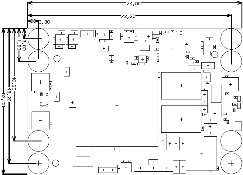
Figure 46: Physical dimensions of the TE0745 SoC module.
Revision History
Hardware Revision History
| Date | Revision | Notes | Link to PCN | Documentation Link |
|---|---|---|---|---|
| 2016-10-11 | 02 |
| - | TE0745-02 |
| 2016-04-18 | 01 |
| - | TE0745-01 |
Table 23: Module hardware revision history.
Hardware revision number is written on the PCB board together with the module model number separated by the dash.
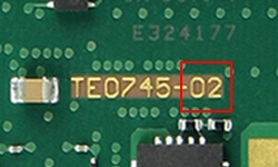
Figure 57: TE0745 module revision number.
Document Change History
| Date | Revision | Contributors | Description | ||||||||
|---|---|---|---|---|---|---|---|---|---|---|---|
| Ali Naseri |
| |||||||||
| 2017-07-19 | v.71 | Ali Naseri, Jan Kumann |
| ||||||||
| 2017-02-05 | v.1V1
| Jan Kumann |
|
Table 24: Document change history.
Disclaimer
| Include Page | ||||
|---|---|---|---|---|
|
Overview
Content Tools