Page History
...
| HTML |
|---|
<!-- Template Revision 1.64 (HTML comments will be not displayed in the document, no need to remove them. For Template/Skeleton changes, increase Template Revision number. So we can check faster, if the TRM style is up to date). --> |
| scroll-ignore | |
|---|---|
| scroll-pdf-ignore | |
Table of Contents
|
Overview
| Scroll Only (inline) |
|---|
Refer to https://wiki.trenz-electronic.de/display/DRAFT/TE0723+TRM for downloadable version of this manual and additional technical documentation of the product.
|
The Trenz Electronic TE0723 is a Arduino compatible FPGA module based on the Xilinx Zynq XC7Z010 SoC.
...
Figure 1: TE0723 block diagram.
Main Components
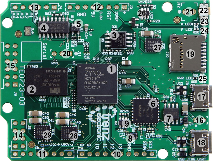
Figure 2: Main components of the TE0723 module.
- Xilinx Zynq XC7Z010 SoC, U1
- 4 Gbit DDR3L 256M x 16 SDRAM, U2
- 16 MByte quad SPI Flash memory, U5
High-speed CMOS logic analog multiplexer/demultiplexer, U10
- 1 MHz low-power operational amplifier, U11
- Dual high-speed USB to multipurpose UART/FIFO, U3
- 0.5A dual-channel current-limited power switch, U21
- Low-power programmable oscillator @ 12.000000 MHz, U7
- 2-Kbit Microwire compatible serial EEPROM, U6
- 10-pin header, J1
- 8-pin header, J2
- 10-pin header, J3
- Analog input header, J4
- 2 x 4-pin header, J5
- PMod 2x6 interface header, J6
- USB host mode jumper, J7
- Micro USB 2.0 Type-B receptacle, J8
- Micro USB 2.0 Type-B receptacle, J9
- Micro SD card connector with detect signal, J10
- Analog input select jumper, J11
- 5V supply power input, J12
- Reset switch, S1
- Red LED, D2
- Green LED, D6
- Green LED, D7
- Ultra-low supply-current voltage monitor, U23
1A PowerSoC DC-DC converter (3.3 V), U20
- 1A PowerSoC DC-DC converter (1.8 V, U19
- 1A PowerSoC DC-DC converter (1.35 V), U16
- Hi-speed USB 2.0 ULPI transceiver, U18
- Low-power programmable oscillator @ 52.000000 MHz, U14
- 1A PowerSoC DC-DC converter (1.0 V), U17
- JTAG interface testpoints, TP1-TP4
Initial Delivery State
Storage device name | IC | Content | Notes |
|---|---|---|---|
Quad SPI Flash | U5 | Empty | - |
| Configuration EEPROM | U6 | Empty | - |
Table 1: Initial delivery state of programmable devices on the module.
Boot Process
The 7 boot mode strapping pins on the TE0723 module are set to boot the system from quad SPI Flash only. For additional information refer to the TE0723 schematic and Xilinx UG585 Zynq-7000 All Programmable SoC Technical Reference Manual (MIO2 ... MIO8) of the Xiliny Zynq Z-7010 device are hardware programmed on the board. They are evaluated by the Zynq device soon after the 'POR_B'.signal is deasserted to begin the boot process (see section "Boot Mode Pin Settings" .You may also refer to this TE0723 reference design for some Boot Process tipsof Xilinx manual UG585).
The TE0723 Zynq board is hardware programmed to boot initially from the on-board QSPI Flash memory U5. The JTAG interface of the module is provided for storing the data to the QSPI Flash memory through the Zynq device.
Signals, Interfaces and Pins
I/O Signals
Overview of the Zynq SoC 's PS/PL banks I/O signals connected to the external connectors:
| Bank | Type | Connector | I/O Signal Count | Voltage | Notes | |
|---|---|---|---|---|---|---|
| 34 | HR | J1 | 8 | 3.3V | Signal Schematic names: 'SCL', 'SDA', 'D8' ... 13, SDA, SCL'D13' | |
| 34 | HR | J2 | 8 | 3.3V | Signal Schematic names: 'RXD', 'TXD', 'D2' .. 7, RXD, TXD. 'D7' | |
| 34 | HR | J6 | 8 | 3.3V | Signal Schematic names: 'PIO01' ... 'PIO08' | |
| 35 | HR | J4 | 6 | 3.3V | Signal Schematic names: 'AIN0' .. 5. 'AIN5' | |
| 35 | HR | J5 | 1 | 3.3V | ESP_GPIO2Connector dedicated to ESP8266 module | |
| 500 | MIO | J10 | 7 | 3.3V | SDCARD | SDIO interface to SD Card socket |
| 501501 | MIO | J5 | 4 | 3.3V | ESP_RXD, ESP_TXD, ESP_GPIO0, MOD_RSTConnector dedicated to ESP8266 module |
Table 2: Overview of the Zynq SoC's PS/PL banks I/O signals
Zynq SoC I/O Banks
| Bank | Type | VCCIO | I/O Signal Count | Available on Connectors | Notes |
|---|---|---|---|---|---|
| 34 | HR | 3.3V | 44 | 24 | 8 user I/O's on Pmod connector J6, female pin header J1 and J2 each. |
| 35 | HR | 3.3V | 8 | 7 | 6 user I/O's on female pin header J4, 1 user I/O on female pin header J5. |
| 500 | PS MIO | 3.3V | 15 | 0 | 6 MIO-pins used for QSPI flash memory interface, 7 MIO-pins used for SD Card interface, 1 MIO-pin connected to red LED D2. |
| 501 | PS MIO | 3.3V | 16 | 4 | 12 MIO-pins used for USB ULPI interface, 4 MIO-pins used for ESP8266 interface header J5. |
| 0 | Config | 3.3V | 5 | 0 | 4 I/O's are dedicated to JTAG interface, 'PROG_B'-signal is connected to voltage monitor circuit 23. |
Table 3: General overview of Zynq SoC PL/PS I/O banks
JTAG Interface
JTAG access to the Xilinx Zynq XC7Z010 SoC is provided through FTDI USB/UART FIFO bridge connected to the J9 Micro USB USB2 connector J9.
Quad SPI Interface
Quad SPI Flash (U5) is connected to the Zynq PS QSPI0 interface via PS MIO bank 500, pins MIO1 ... MIO6.
| Zynq SoC's MIOPin | Signal Name | U5 Pin |
|---|---|---|
| 1Bank 500, pin MIO1 | SPI0_CS | 1 |
| 2Bank 500, pin MIO2 | SPI0_DQ0/MIO2 | 53 |
| Bank 500, pin MIO3 | SPI0_DQ1/MIO3 | 24 |
| Bank 500, pin MIO4 | SPI0_DQ2/MIO4 | 35 |
| Bank 500, pin MIO5 | SPI0_DQ3/MIO5 | 7 |
| 6Bank 500, pin MIO6 | SPI0_SCK | 6 |
Table 34: Quad SPI interface signals and connections.
SD Card Interface
TE0723 module has on-board 3.3V SD Card socket (J10) with card detect switch wired to the SoC PS MIO bank 500.
| Zynq SoC's Pin | Connected To | Signal Name |
|---|---|---|
| Bank 500, pin MIO0 | J10-9 | Card detect switch |
| Bank 500, pin MIO10 | J10-7 | DAT0 |
| Bank 500, pin MIO11 | J10-3 | CMD |
| Bank 500, pin MIO12 | J10-5 | CLK |
| Bank 500, pin MIO13 | J10-8 | DAT1 |
| Bank 500, pin MIO14 | J10-1 | DAT3 |
| Bank 500, pin MIO15 | J10-2 | CD/DAT3 |
Table 4: SD card socket signals.
USB Interface
| Zynq SoC's Pin | Connected To | Signal Name |
|---|---|---|
| Bank 501, pin MIO28 | U18-7 | OTG-DATA4 |
| Bank 501, pin MIO29 | U18-31 | OTG-DIR |
| Bank 501, pin MIO30 | U18-29 | OTG-STP |
| Bank 501, pin MIO31 | U18-2 | OTG-NXT |
| Bank 501, pin MIO32 | U18-3 | OTG-DATA0 |
| Bank 501, pin MIO33 | U18-4 | OTG-DATA1 |
| Bank 501, pin MIO34 | U18-5 | OTG-DATA2 |
| Bank 501, pin MIO35 | U18-6 | OTG-DATA3 |
| Bank 501, pin MIO36 | U18-1 | OTG-CLK |
| Bank 501, pin MIO37 | U18-9 | OTG-DATA5 |
| Bank 501, pin MIO38 | U18-10 | OTG-DATA6 |
| Bank 501, pin MIO39 | U18-13 | OTG-DATA7 |
Table 5: USB interface.
...
| Zynq SoC's Pin | Connected To | Signal Name |
|---|---|---|
| Bank 501, pin MIO48 | J5-2 | ESP_TXD |
| Bank 501, pin MIO49 | J5-7 | ESP_RXD |
| Bank 501, pin MIO52 | J5-6 | MOD_RST |
| Bank 501, pin MIO53 | J5-3 | ESP_GPIO0 |
| Bank 35, pin G15 | J5-5 | ESP_GPIO2 |
Table 6: ESP8266 Wi-Fi module interface.
...
Overview
Content Tools