Page History
...
| Scroll Only (inline) |
|---|
Refer to https://wiki.trenz-electronic.de/display/DRAFTPD/TE0723+TRM for downloadable version of this manual and additional technical documentation of the product. |
...
Figure 1: TE0723 block diagram
Main Components
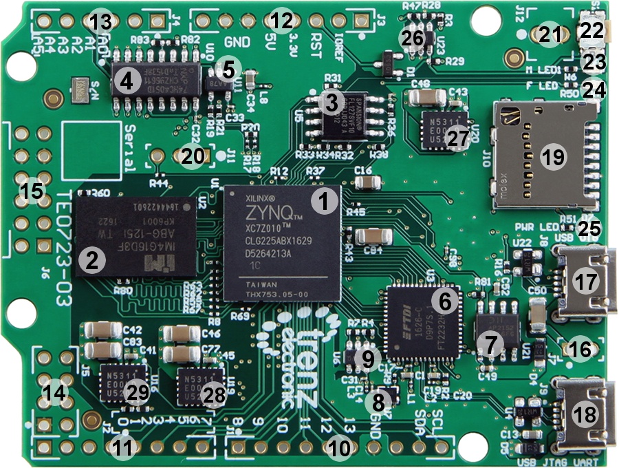
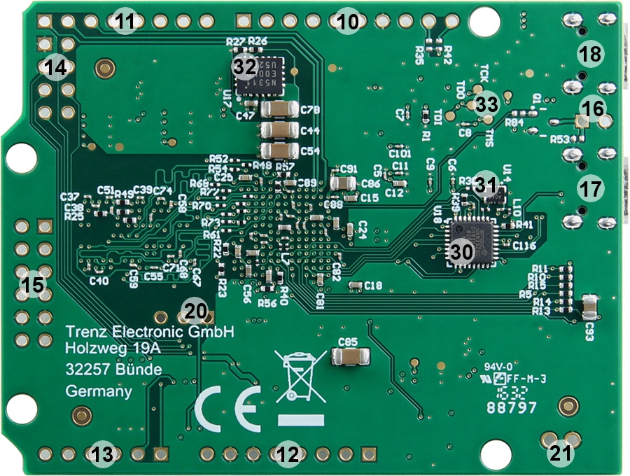
Figure 2: Main components of the TE0723 module
...
Signals, Interfaces and Pins
I/O Signals on Connectors
Overview of the Zynq SoC PS/PL banks I/O signals connected to the external connectors:
...
Table 2: Overview of the Zynq SoC's PS/PL banks I/O signals
Zynq SoC I/O Banks
| Bank | Type | VCCIO | I/O Signal Count | Available on Connectors | Notes |
|---|---|---|---|---|---|
| 34 | HR | 3.3V | 44 | 24 | 8 user I/O's on Pmod connector J6, female pin header J1 and J2 each. |
| 35 | HR | 3.3V | 8 | 7 | 6 user I/O's on female pin header J4, 1 user I/O on female pin header J5. |
| 500 | PS MIO | 3.3V | 15 |
| - | 6 MIO-pins used for QSPI flash memory interface, 7 MIO-pins used for SD Card interface, 1 MIO-pin connected to red LED D2. | ||||
| 501 | PS MIO | 3.3V | 16 | 4 | 12 MIO-pins used for USB ULPI interface, 4 MIO-pins used for ESP8266 interface header J5. |
| 0 | Config | 3.3V | 5 |
| - | 4 I/O's are dedicated to JTAG interface, 'PROG_B'-signal is connected to voltage monitor circuit 23. |
Table 3: General overview of Zynq SoC PL/PS I/O banks
...
JTAG access to the Xilinx Zynq XC7Z010 SoC is provided through FTDI USB/UART FIFO bridge connected to the Micro USB2 connector J9.
Quad SPI Interface
USB to JTAG/UART
The TE0723 board is equipped with the FTDI FT2232H USB2 to JTAG/UART adapter controller connected to micro-USB2 connector J9 to provide JTAG and UART access to the Xilinx Zynq XC7Z010 SoC. There is also a 256-byte configuration EEPROM U6 wired to the FT2232H chip via Microwire bus which holds pre-programmed license code to support Xilinx programming tools.
| Warning |
|---|
Do not access the FT2232H EEPROM using FTDI programming tools, doing so will erase normally invisible user EEPROM content and invalidate stored Xilinx JTAG license. Without this license the on-board JTAG will not be accessible any more with any Xilinx tools. Software tools from FTDI website do not warn or ask for confirmation before erasing user EEPROM content. |
Channel A of the FTDI IC is configured as JTAG interface (MPSSE) connected to the JTAG interface of the Zynq SoC:
Signal Schematic Name | FT2232H IC U3 | Zynq SoC U1 | Note |
|---|---|---|---|
| TCK | Pin 12 | Pin G9 | - |
| TDI | Pin 13 | Pin L7 | - |
| TDO | Pin 14 | Pin L8 | - |
| TMS | Pin 15 | Pin L9 | - |
Table 4: JTAG interface signals
Channel B of the FTDI IC can be used as UART interface routed to CPLD. Also 6 additional bus-lanes are connected to the System Controller CPLD and available for user-specific use.
Signal Schematic Name | FT2232H IC U3 | Zynq SoC U1 | Note |
|---|---|---|---|
| BDBUS0 | Pin 12 | Pin G9 | - |
| TDI | Pin 13 | Pin L7 | - |
| TDO | Pin 14 | Pin L8 | - |
| TMS | Pin 15 | Pin L9 | - |
Table 5: JTAG interface signals
Quad SPI Interface
Quad SPI Flash (U5) is connected to the Zynq PS QSPI0 interface via PS Quad SPI Flash (U5) is connected to the Zynq PS QSPI0 interface via PS MIO bank 500, pins MIO1 ... MIO6.
...
Table 6: ESP8266 Wi-Fi module interface.
...
I²C Interface
I2C interface pins SCL and SDA from the Zynq SoC PL bank 34 are connected to the connector J1. There are no on-board I2C slave devices.
...
Overview
Content Tools