Page History
...
| Scroll Title | ||||||||||||||||||||||||
|---|---|---|---|---|---|---|---|---|---|---|---|---|---|---|---|---|---|---|---|---|---|---|---|---|
| ||||||||||||||||||||||||
|
Main Components
| Scroll Title | ||||||||||||||||||||||||
|---|---|---|---|---|---|---|---|---|---|---|---|---|---|---|---|---|---|---|---|---|---|---|---|---|
| ||||||||||||||||||||||||
|

Photo shows similar TE0841-01
- Xilinx Kintex UltraScale FPGA, U1
- Ultra performance oscillator @25.000000 MHz, U3
- 12A PowerSoC DC-DC converter (0.95V), U14
- 12A PowerSoC DC-DC converter (0.95V), U7
Low-jitter precision LVDS oscillator @200.0000 MHz, U11
- Low-dropout (LDO) linear regulator (MGTAVTT 1.20V), U8
- Low-dropout (LDO) linear regulator (MGTAVCC 1.02V), U12
- Samtec Razor Beam™ LSHM-150 B2B connector, JM1
- Samtec Razor Beam™ LSHM-150 B2B connector, JM2
- Samtec Razor Beam™ LSHM-130 B2B connector, JM3
- Programmable quad clock generator, U2
- 64 MByte QSPI Flash, U6
- 8 Gbit DDR4 SDRAM, U4
- 8 Gbit DDR4 SDRAM, U5
- System Controller CPLD, U18
- Low-dropout (LDO) linear regulator (MGTAUX), U9
- Ultra-low power low-dropout (LDO) regulator (VBATT), U19
Initial Delivery State
Storage device name | Content | Notes |
|---|---|---|
System Controller CPLD | Default firmware | - |
| OTP Flash area | Empty | Not programmed |
| Quad clock generator OTP area | Empty | Not programmed |
Table 1: TE0841-02 module initial delivery state of programmable on-board devices
...
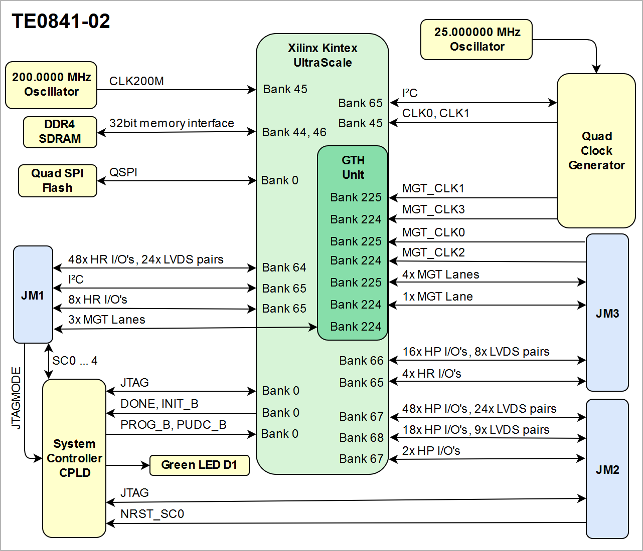
I/O signals connected to the SoCs I/O bank and B2B connector:
| FPGA Bank | Type | B2B Connector | I/O Signal Count | Bank VCCO Voltage | Notes |
|---|---|---|---|---|---|
| 64 | HR | JM1 | 48 IO's, 24 LVDS pairs | B64_VCCO | Supplied by the carrier board |
| 65 | HR | JM1 | 8 IO's | 3.3V | On-module power supply |
| 65 | HR | JM3 | 4 IO's | 3.3V | On-module power supply |
| 66 | HP | JM3 | 16 IO's, 8 LVDS pairs | B66_VCCO | Supplied by the carrier board |
| 67 | HP | JM2 | 48 IO's, 24 LVDS pairs | B67_VCCO | Supplied by the carrier board |
| 67 | HP | JM2 | 2 IO's | B67_VCCO | Supplied by the carrier board |
| 68 | HP | JM2 | 18 IO's, 9 LVDS pairs | B68_VCCO | Supplied by the carrier board |
Table 2: General overview of FPGA's PL I/O signals connected to the B2B connectors
...
MGT (Multi Gigabit Transceiver) lane consists of one transmit and one receive (TX/RX) differential pairs, two signals each or four signals total per one MGT lane. Following table lists lane number, MGT bank number, transceiver type, signal schematic name, board-to-board pin connection and FPGA pins connection:
| Lane | Bank | Type | Signal Name | B2B Pin | FPGA Pin |
|---|---|---|---|---|---|
| 0 | 225 | GTH |
|
|
|
| 1 | 225 | GTH |
|
|
|
| 2 | 225 | GTH |
|
|
|
| 3 | 225 | GTH |
|
|
|
| 4 | 224 | GTH |
|
|
|
| 5 | 224 | GTH |
|
|
|
| 6 | 224 | GTH |
|
|
|
| 7 | 224 | GTH |
|
|
|
Table 3: FPGA to B2B connectors routed MGT lanes overview
Below are listed MGT banks reference clock sources:
| Clock signal | Bank | Source | FPGA Pin | Notes |
|---|---|---|---|---|
| MGT_CLK0_P | 225 | B2B, JM3-33 | MGTREFCLK0P_225, Y6 | Supplied by the carrier board. |
| MGT_CLK0_N | B2B, JM3-31 | MGTREFCLK0N_225, Y5 | ||
| MGT_CLK1_P | 225 | U2, CLK1B | MGTREFCLK1P_225, V6 | On-board Si5338A. |
| MGT_CLK1_N | U2, CLK1A | MGTREFCLK1N_225, V5 | ||
| MGT_CLK2_P | 224 | B2B, JM3-34 | MGTREFCLK2P_224, AD6 | Supplied by the carrier board. |
| MGT_CLK2_N | B2B, JM3-32 | MGTREFCLK2N_224, AD5 | ||
| MGT_CLK3_P | 224 | U2, CLK2B | MGTREFCLK3P_224, AB6 | On-board Si5338A. |
| MGT_CLK3_N | U2, CLK2B | MGTREFCLK3N_224, AB5 |
Table 4: MGT reference clock sources
...
JTAG access to the Xilinx Kintex UltraScale FPGA is available through B2B connector JM2.
JTAG Signal | B2B Connector Pin |
|---|---|
| TMS | JM2-93 |
| TDI | JM2-95 |
| TDO | JM2-97 |
| TCK | JM2-99 |
Table 5: JTAG interface signals
...
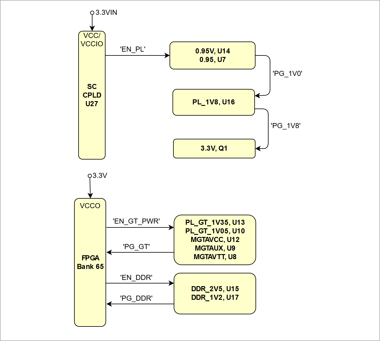
Special purpose pins are connected to the System Controller CPLD and have following default configuration:
| Pin Name | SC CPLD Direction | Function | Default Configuration |
|---|---|---|---|
| JTAGMODE | Input | JTAG select | Low for normal operation. |
| nRST_SC0 | Input | Reset | Low active board reset input |
| SC1 | - | - | not currently used ('BOOTMODE' in default B2B pin out') |
| SC2 | Input / Output | - | Power good signal ('PGOOD' in default B2B pin out) |
| SC3 | Input | - | Power enable pin ('EN1' in default B2B pin out) |
| SC4 | - | - | not currently used ('NOSEQ' in default B2B pin out') |
| F_TCK | Output | JTAG signals between | B2B JTAG signals are forwarded to the FPGA through SC CPLD. |
| F_TMS | Output | ||
| F_TDI | Output | ||
| F_TDO | Input | ||
| TCK | Input | JTAG signals between SC CPLD and B2B connector | Program FPGA or SC CPLD depending on pin JTAGMODE. |
| TMS | Input | ||
| TDI | Input | ||
| TDO | Output | ||
| PROG_B | Output | FPGA configuration | PL configuration reset signal. |
| DONE | Input | FPGA configuration done | PL configuration completed. |
| PUDC_B | Output | Pull up during configuration | PL I/O's are 3-stated until configuration of the FPGA completes. |
| INIT_B | Input | Initialization done | Low active FPGA initialization pin or configuration error signal. |
| EN_PL | Input | Enable PL Power DC-DC converters | Set to contant logical high. |
| CPLD_IO | Output | user I/O | Connected to FPGA Bank 45, pin P28. |
Table 6: System Controller CPLD I/O pins
...
Quad SPI interface is connected to the FPGA configuration bank 0.
| Signal Name | QSPI Flash Memory U6 Pin | FPGA Pin |
|---|---|---|
| SPI_CS | C2 | RDWR_FCS_B_0, AH7 |
| SPI_D0 | D3 | D00_MOSI_0, AA7 |
| SPI_D1 | D2 | D01_DIN_0, Y7 |
| SPI_D2 | C4 | D02_0, U7 |
| SPI_D3 | D4 | D03_0, V7 |
| SPI_CLK | B2 | CCLK_0, V11 |
Table 7: Quad SPI interface signals and connections
...
On-module I²C interface is routed from PL bank 65 I/O pins (PLL_SCL and PLL_SDA) to the I²C interface of Si5338 PLL quad clock generator U2, also two further pins of bank 65 can be used as external I²C interface of the modue:
| I²C Interface | Schematic net names | Connected to | I²C Address | Notes |
|---|---|---|---|---|
| PL bank 65 I/O | 'PLL_SCL', pin AB20 'PLL_SDA' pin AB19 | Si5338 U2, pin 12 Si5338 U2, pin 19 | 0x70 | default address |
| PL bank 65 I/O | 'B65_SCL', pin Y19 'B65_SDA', pin AA19 | B2B JM1, pin 95 B2B JM1, pin 93 | - |
Table 8: I2C slave device addresses
...
There is a Silicon Labs I2C programmable quad PLL clock generator on-board (Si5338A, U2) to generate various reference clocks for the module.
| Si5338A Pin | Signal Name / Description | Connected to | Direction | Note |
|---|---|---|---|---|
IN1 | - | not connected | Input | not used |
| IN2 | - | GND | Input | not used |
IN3 | Reference input clock | U3, pin 3 | Input | 25.000000 MHz oscillator, Si8208AI |
IN4 | - | GND | Input | I2C slave device address LSB. |
IN5 | - | not connected | Input | not used |
| IN6 | - | GND | Input | not used |
CLK0A | CLK1_P | U1, R23 | Output | FPGA bank 45, default 100MHz* |
| CLK0B | CLK1_N | U1, P23 | ||
| CLK1A | MGT_CLK1_N | U1, V5 | Output | FPGA MGT bank 225 reference clock, default 125MHz* |
| CLK1B | MGT_CLK1_P | U1, V6 | ||
| CLK2A | MGT_CLK3_N | U1, AB5 | Output | FPGA MGT bank 224 reference clock, default 156,25MHz* |
| CLK2B | MGT_CLK3_P | U1, AB6 | ||
| CLK3A | CLK0_P | U1, pin T24 | Output | FPGA bank 45, default 156,25MHz* |
| CLK3B | CLK0_N | U1, pin T25 |
Table 9: Programmable quad PLL clock generator inputs and outputs, *PCB REV01 is not programmed
...
The FPGA module has following reference clocking signals provided by external baseboard sources and on-board oscillators:
| Clock Source | Frequency | Signal Name | Clock Destination | Notes |
|---|---|---|---|---|
| U3, SiT8208AI | 25.000000 MHz | CLK | Si5338A PLL U2, pin 3 (IN3) | - |
| U11, DSC1123DL5 | 200.0000 MHz | CLK200M_P | FPGA bank 45, pin R25 | Enable by FPGA bank 65, pin AF24 Signal: 'ENOSC' |
| CLK200M_N | FPGA bank 45, pin R26 |
Table 10: Reference clock signals
On-board LEDs
| LED | Color | Connected to | Description and Notes |
|---|---|---|---|
| D1 | Green | System Controller CPLD, bank 3 | Exact function is defined by SC CPLD firmware. |
Table 11: On-board LEDs
Power and Power-On Sequence
...
Xilinx provide a power estimator excel sheets to calculate power consumption. It's also possible to evaluate the power consumption of the developed design with Vivado. See also Trenz Electronic Wiki FAQ.
| Power Input | Typical Current |
|---|---|
| VIN | TBD* |
| 3.3VIN | TBD* |
Table 12: Typical power consumption
...
| Scroll Title | ||||||||||||||||||||||||
|---|---|---|---|---|---|---|---|---|---|---|---|---|---|---|---|---|---|---|---|---|---|---|---|---|
| ||||||||||||||||||||||||
|
See also Xilinx datasheet DS892 for additional information. User should also check related base board documentation when intending base board design for TE0841 module.
...
| Scroll Title | ||||||||||||||||||||||||
|---|---|---|---|---|---|---|---|---|---|---|---|---|---|---|---|---|---|---|---|---|---|---|---|---|
| ||||||||||||||||||||||||
|
Power Rails
| Power Rail Name | B2B JM1 Pins | B2B JM2 Pins | Input/Output | Notes |
|---|---|---|---|---|
| VIN | 1, 3, 5 | 2, 4, 6, 8 | Input | Supply voltage. |
| 3.3VIN | 13, 15 | - | Input | Supply voltage. |
| B64_VCO | 9, 11 | - | Input | HR (High Range) bank voltage. |
| B66_VCO | - | 1, 3 | Input | HP (High Performance) bank voltage. |
| B67_VCO | - | 7, 9 | Input | HP (High Performance) bank voltage. |
| B68_VCO | - | 5 | Input | HP (High Performance) bank voltage. |
VBAT_IN | 79 | - | Input | RTC battery supply voltage. |
| 3.3V | - | 10, 12, 91 | Output | Module on-board 3.3V voltage level. |
Table 13: Module power rails
| Note |
|---|
Current rating of Samtec Razor Beam™ LSHM B2B connectors is 2.0A per pin (2 adjacent pins powered). |
Bank Voltages
Bank | Schematic Name | Voltage | Voltage Range |
|---|---|---|---|
| 0 (config) | PL_1.8V | 1.8V | - |
| 44 HP | DDR_1V2 | 1.2V | HP: 1.2V to 1.8V |
| 45 HP | PL_1.8V | 1.8V | HP: 1.2V to 1.8V |
| 46 HP | DDR_1V2 | 1.2V | HP: 1.2V to 1.8V |
| 64 HR | B64_VCO | user | HR: 1.2V to 3.3V |
| 65 HR | 3.3V | 3.3V | HR: 1.2V to 3.3V |
| 66 HP | B66_VCO | user | HP: 1.2V to 1.8V |
| 67 HP | B67_VCO | user | HP: 1.2V to 1.8V |
| 68 HP | B68_VCO | user | HP: 1.2V to 1.8V |
Table 14: Module PL I/O bank voltages
...
See also the current available variants on the Trenz Electronic shop page
| Trenz shop TE0841 overview page | |
|---|---|
| English page | German page |
Technical Specifications
Absolute Maximum Ratings
Parameter | Min | Max | Units | Reference Document |
|---|---|---|---|---|
VIN supply voltage | -0.3 | 6.0 | V | EN63A0QI, TPS74401RGW datasheets |
| 3.3VIN supply voltage | -0.1 | 3.4 | V | Xilinx datasheet DS892 (HR Bank VCCO) |
| VBAT_IN | -0.3 | 6.0 | V | TPS780xx datasheet |
| Supply voltage for HR I/O banks (VCCO) | -0.500 | 3.400 | V | Xilinx datasheet DS892 |
Supply voltage for HP I/O banks (VCCO) | -0.500 | 2.000 | V | Xilinx datasheet DS892 |
| I/O input voltage for HR I/O banks | -0.400 | VCCO + 0.550 | V | Xilinx datasheet DS892 |
I/O input voltage for HP I/O banks | -0.550 | VCCO + 0.550 | V | Xilinx datasheet DS892 |
| GTH and GTY transceiver reference clocks absolute input voltage (MGT_CLK0, MGT_CLK2) | -0.500 | 1.320 | V | Xilinx datasheet DS892 |
GTH and GTY transceiver receiver (RXP/RXN) and transmitter (TXP/TXN) absolute input voltage | -0.500 | 1.260 | V | Xilinx datasheet DS892 |
Storage temperature | -40 | +100 | °C | SML-P11 LED datasheet |
Table 16: Module absolute maximum ratings
...
Recommended Operating Conditions
| Parameter | Min | Max | Units | Reference Document |
|---|---|---|---|---|
| VIN supply voltage | 3.3 | 5.5 | V | TPS82085SIL, TPS74401RGW datasheet |
| 3.3VIN supply voltage | 3.3 | 3.4 | V | Xilinx datasheet DS892 (HR Bank VCCO) |
| VBAT_IN | 2.2 | 5.5 | V | TPS780xx datasheet |
| Supply voltage for HR I/O banks (VCCO) | 1.140 | 3.400 | V | Xilinx datasheet DS892 |
Supply voltage for HP I/O banks (VCCO) | 0.950 | 1.890 | V | Xilinx datasheet DS892 |
I/O input voltage for HR I/O banks | –0.200 | VCCO + 0.20 | V | Xilinx datasheet DS892 |
| I/O input voltage for HP I/O banks | –0.200 | VCCO + 0.20 | V | Xilinx datasheet DS892 |
| I/O input voltage for SC CPLD U18 | -0.3 | 3.6 | V | LCMXO2-256HC datasheet |
Industrial Module Operating Temperature Range | -40 | 85 | °C | Xilinx datasheet DS892 |
| Commercial Module Operating Temperature Range | 0 | 85 | Xilinx DS892, Silicon Labs Si5338 datasheet |
Table 17: Module recommended operating conditions
...
Hardware Revision History
| Date | Revision | Notes | PCN | Documentation Link |
|---|---|---|---|---|
| 2018-05-11 | 02 | current available board revision | PCN-20180511 | TE0841-02 |
| 2015-12-09 | 01 | First production release | - | TE0841-01 |
Table 18: Module hardware revision history
...
Overview
Content Tools