Page History
...
- Xilinx Kintex-7 XC7K160T, XC7K325T or XC7K410T FPGA SoC
- Large number of configurable I/Os are provided via rugged HPC FMC connector
- Dual ARM Cortex-A9 MPCore
- 1 GByte RAM (32-Bit wide DDR3)
- 32 MByte QSPI Flash memory
- 2 x Hi-Speed USB2 ULPI transceiver PHY
- 2 x Gigabit (10/100/1000 Mbps) Ethernet transceiver PHY
- 4 GByte eMMC (optional up to 64 GByte)
- 2 x MAC-address EEPROMs
- Optional 2x 64 MByte HyperFLASH or 2x 8 MByte HyperRAM (max 2x 32 MByte HyperRAM)
- Temperature compensated RTC (real-time clock)
- Si5338A programmable quad PLL clock generator for GTX transceiver clocks
- Plug-on module with 3 x 160-pin high-speed strips
- 16 GTX high-performance transceiver
- 2x GT transceiver clock inputs
- 254 FPGA I/O's (125 LVDS pairs)
- On-board high-efficiency switch-mode DC-DC converters
- System management
- eFUSE bit-stream encryption
- AES bit-stream encryption
- Evenly-spread supply pins for good signal integrity
- User LED
...
- PCI Express 2.0 x8 card with maximum throughput of 4 GB/s
- FMC High Pin Count (HPC) connector
- 8 FPGA MGT lanes available on PCIe interface
- DDR3 SO-DIMM SDRAM socket
- 256-Mbit (32-MByte) Quad SPI Flash memory (for configuration and operation) accessible through:
- FPGA
- JTAG port (SPI indirect, bus width x4)
- External clock input via SMA coaxial connector
- 28 GTH transceivers, each with up to 13.1 Gbit/s data transmission rate
- FPGA configuration through:
- JTAG connector
- Quad SPI Flash memory
- Programmable quad clock generator
TI LMK04828B ultra low-noise JESD204B compliant clock jitter cleaner
- On-board high-efficiency DC-DC converters
- Up to 202 FPGA I/O pins available on FMC connector (up to 101 LVDS pairs possible)
- System management and power sequencing
- AES bit-stream encryption
- eFUSE bit-stream encryption
- Xilinx Kintex UltraScale FPGA (XCKU035 or XCKU040)
- 2 banks of 1024 MByte DDR4 SDRAM, 32bit wide memory interface
- 512 Mbit (64 MByte) QSPI Flash
- 3 x Samtec Razor Beam LSHM B2B, 260 terminals total
- 60 x HR I/Os
- 84 x HP I/Os
- 8 x GTH transceiver lanes (TX/RX)
- 2 x MGT external clock inputs - Clocking
- Si5338 - 4 output PLLs, GT and PL clocks
- 200 MHz LVDS oscillator - All power supplies on-board, single power source operation
- Evenly spread supply pins for optimized signal integrity
- Size: 40 x 50 mm
- 3 mm mounting holes for skyline heat spreader
- Rugged for industrial applications
Additional assembly options are available for cost or performance optimization upon request.
Block Diagram
| HTML |
|---|
<!--
Rules for all diagrams:
1. All diagrams are wrapped in the "Scroll Title" macro.
	- The title has to be named with the diagrams name
	- The anchor has the designation figure_x, whereby x is the number of the diagram

2. The Draw.IO diagram has to be inserted in the "Scroll Ignore" macro
	- Border has to be switched off in the macro edit
	- Toolbar has to be hidden in the macro edit

3. A PNG Export of the diagram has to be inserted in the "Scroll Only" macro, see Wiki page "Diagram Drawing Guidelines" how to do this step.

The workaround with the additional PNG of the diagram is necessary until the bug of the Scroll PDF Exporter, which cuts diagram to two pages, is fixed.


IMPORTANT NOTE: In case of copy and paste the TRM skeleton to a new Wiki page, delete the Draw.IO diagrams and the PNGs, otherwise due to the linkage of the copied diagrams every change in the TRM Skeleton will effect also in the created TRM and vice versa!

See page "Diagram Drawing Guidelines" how to clone an existing diagram as suitable template for the new diagram!

--> |
| Scroll Title | ||||||||||||||||||||||||||||||||
|---|---|---|---|---|---|---|---|---|---|---|---|---|---|---|---|---|---|---|---|---|---|---|---|---|---|---|---|---|---|---|---|---|
| ||||||||||||||||||||||||||||||||
|
Main Components
| Scroll Title | ||||||||||||||||||||||||||||||||
|---|---|---|---|---|---|---|---|---|---|---|---|---|---|---|---|---|---|---|---|---|---|---|---|---|---|---|---|---|---|---|---|---|
| ||||||||||||||||||||||||||||||||
|
- Xilinx Kintex XC7K-2FBG676I FPGA SoC, U6
- ANSI/VITA 57.1 compliant FMC HPC connector, J2
Block Diagram
| HTML |
|---|
<!--
Rules for all diagrams:
1. All diagrams are wrapped in the "Scroll Title" macro.
	- The title has to be named with the diagrams name
	- The anchor has the designation figure_x, whereby x is the number of the diagram

2. The Draw.IO diagram has to be inserted in the "Scroll Ignore" macro
	- Border has to be switched off in the macro edit
	- Toolbar has to be hidden in the macro edit

3. A PNG Export of the diagram has to be inserted in the "Scroll Only" macro, see Wiki page "Diagram Drawing Guidelines" how to do this step.

The workaround with the additional PNG of the diagram is necessary until the bug of the Scroll PDF Exporter, which cuts diagram to two pages, is fixed.


IMPORTANT NOTE: In case of copy and paste the TRM skeleton to a new Wiki page, delete the Draw.IO diagrams and the PNGs, otherwise due to the linkage of the copied diagrams every change in the TRM Skeleton will effect also in the created TRM and vice versa!

See page "Diagram Drawing Guidelines" how to clone an existing diagram as suitable template for the new diagram!

--> |
...
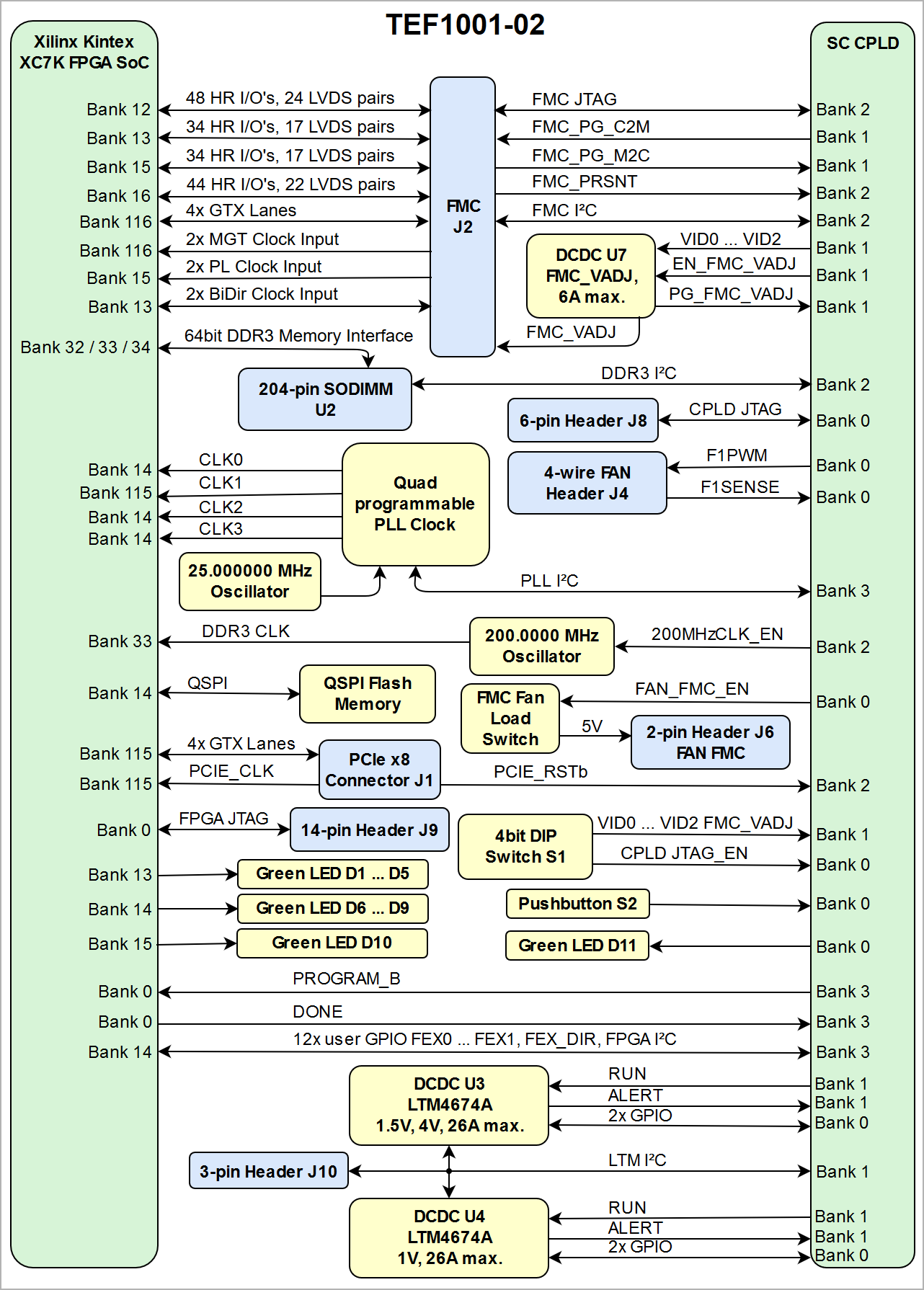
| anchor | Figure_1 |
|---|---|
| title | Figure 1: TEF1001-02 block diagram |
...
| Scroll Only |
|---|
|
Main Components
...
| anchor | Figure_2 |
|---|---|
| title | Figure 2: TEF1001-02 main components |
...
| Scroll Only |
|---|
|
- Xilinx Kintex XC7K-2FBG676I FPGA SoC, U6
- ANSI/VITA 57.1 compliant FMC HPC connector, J2
- Cooling fan 5VDC M1 (45X5MM, 0.7W, 1.06CFM), M1
- PCIe x8 connector, J1
- SO-DIMM socket, U2
- 6-pin 12V power connector, J5
- Step-down DC-DC converter @1.5V and @4V (LT LTM4676A), U3
- Step-down DC-DC converter @1.0V (LT LTM4676A), U4
- 256 Mbit Quad SPI Flash Memory (Micron N25Q256A), U12
- 10x Green user LEDs, D1 ... D10
- 4-wire PWM fan connector, J4
- User button, S2
- FPGA JTAG connector, J9
- sd
- sd
- sd
- sd
- s
- sd
- sd
- s
- sd
- sd
- s
- s
- sd
- sd
- sd
- sd
- FPGA JTAG connector, J9
- User button, S2
- SO-DIMM socket, U2
- Xilinx Virtex-7 XC7VX330T-2FFG1157C FPGA, U1
- ANSI/VITA 57.1 compliant FMC HPC connector, J2
- SMA coaxial connector for external clock input, J3
- System Controller CPLD JTAG connector, J8
- I2C connector for LT LTM4676 step-down DC-DC regulator, J10
- IDC header for access to 5 x high-speed data lanes (LVDS pairs), J7
- 4-wire PWM fan connector, J4
- 6-pin 12V power connector, J5
- Reference clock generator @10.0 MHz (P5146) , U11
- LDO DC-DC regulator @3.3V (LMK_3V3) (TI TPS74901RGWR), U21
- 256 Mbit Quad SPI Flash Memory (Micron N25Q256A), U12
- Cooling fan 5VDC M1 (45X5MM, 0.7W, 1.06CFM)
- System Controller CPLD (Lattice Semiconductor LCMXO2-1200HC), U5
- , M1
- PCIe x8 connector, J1
- SO-DIMM socket, U2
- 6-pin 12V power connector, J5Ultra low jitter clock synthesizer (TI LMK04828B), U9
- Step-down DC-DC regulator converter @1.0V 5V and @4V (LT LTM4676LTM4676A), U4U3
- Step-down DC-DC regulator converter @1.5V 0V (VCC1V5LT LTM4676A) (LT LTM4676, U3
- I2C Programmable quad clock generator (Silicon Labs Si5338A), U13
- 4A PowerSoC DC-DC converter @1.8V (Altera EN6347QI, U20
- LDO DC-DC regulator @1.0V (MGTAVCC_FPGA) (TI TPS74401RGW), U18
- LDO DC-DC regulator @1.2V (MGTAVTT_FPGA) (TI TPS74401RGW), U17
- U4
- 256 Mbit Quad SPI Flash Memory (Micron N25Q256A), U12
- 10x Green user LEDs connected to FPGA, D1 ... D10
- 4-wire PWM fan connector, J4
- User button, S2
- FPGA JTAG connector, J9
- 4bit DIP switch, S1
- I²C header for LTM4676A DC-DC converter, J10
- System Controller CPLD JTAG header, J8
- 1x Green LED connected to SC CPLD, D11
- 2-pin 5V FAN header, J6
- System Controller CPLD (Lattice Semiconductor LCMXO2-1200HC), U5
- 6A PowerSoC DC-DC converter @FMC_VADJ (Altera EN5365QI), U7
- 4A PowerSoC DC-DC converter 4A PowerSoC DC-DC converter @3.3V (3V3FMC) (Altera EN6347QI), U15
- LDO converter @1.2V (MGTAVTT_FPGA) (TI TPS74401RGW), U17
- LDO converter @1.0V (MGTAVCC_FPGA) (TI TPS74401RGW), U18
- 4A PowerSoC DC-DC converter @1.8V (FMC_VADJ) (Altera EN6347QI), U7
Initial Delivery State
| Storage device name | Content | Notes | ||||
|---|---|---|---|---|---|---|
| 24LC128-I/ST | not programmed | User content | ||||
24AA025E48 EEPROM's | User content not programmedValid MAC Address from manufacturer | |||||
| Si5338A OTP Area | not programmed | -eMMC | ||||
SPI Flash | MemoryOTP Area | Empty, not programmed | Except serial number programmed by flash vendor | |||
SPI Flash OTP Area | Empty, not programmed | Except serial number programmed by flash vendor | Quad Enable bit | SPI Flash Quad Enable bit | Programmed | - |
SPI Flash main array | demo design | - | ||||
| HyperFlash Memory | not programmed | - | ||||
eFUSE USER | Not programmed | - | ||||
eFUSE Security | Not programmed | - |
Table 1: Initial delivery state of programmable devices on the module
Boot Process
4 of the 7 boot mode strapping pins (MIO2 ... MIO8) of the Xilinx Zynq-7000 SoC device are hardware programmed on the board, 3 of them are set by the SC CPLD firmware. The boot strapping pins are evaluated by the Zynq device soon after the 'PS_POR' signal is deasserted to begin the boot process (see section "Boot Mode Pin Settings" of Xilinx manual UG585).
The TE0782 board is programmed in the SC CPLD firmware to boot initially from the on-board QSPI Flash memory U38. See section Bootmode in the TE0782 SC CPLD reference Wiki page.
The JTAG interface of the module is provided for storing the data to the QSPI Flash memory through the Zynq-7000 device.
Signals, Interfaces and Pins
Board to Board (B2B) I/Os
Zynq-7000 SoC's I/O banks signals connected to the B2B connectors:
By default the configuration mode pins M[2:0] of the FPGA are set to QSPI mode (Master SPI), hence the FPGA is configured from serial NOR flash at system start-up. The JTAG interface of the module is provided for storing the initial FPGA configuration data to the QSPI flash memory.
Signals, Interfaces and Pins
| HTML |
|---|
<!--
Connections and Interfaces or B2B Pin's which are accessible by User
--> |
FMC HPC Connector I/Os
I/O signals connected to the SoCs I/O bank and B2B connector:
| FPGA Bank | Type |
|---|
| I/O Signal Count |
|---|
| Bank VCCO Voltage | Notes |
|---|
| 64 | HR |
J3
44
User
11
HR
J3
40
User
HR
J2
40
User
13
HR
J2
40
User
33
HP
J1
48
User
| 48 IO's, 24 LVDS pairs | B64_VCCO | Supplied by the carrier board | ||
| 65 | HR | 8 IO's | 3.3V | On-module power supply |
| 65 | HR | 4 IO's | 3.3V | On-module power supply |
| 66 | HP | 16 IO's, 8 LVDS pairs | B66_VCCO | Supplied by the carrier board |
| 67 | HP | 48 IO's, 24 LVDS pairs | B67_VCCO | Supplied by the carrier board |
| 67 | HP | 2 IO's | B67_VCCO | Supplied by the carrier board |
| 68 | HP | 18 IO's, 9 LVDS pairs | B68_VCCO | Supplied by the carrier board |
Table 2: General overview of board to board FPGA's PL I/O signals connected to the FMC connector
For detailed information about the pin - out, please refer to the Pin-out tableTables.
MGT Lanes
| HTML |
|---|
<!--
TO-DO (future):
If Vivado board part files are available for this module, the standard configuration of the MIO pins by using this board part files should be mentioned here. This standard configuration of those pins are also apparent of the on-board peripherals of base-boards related to the module.
--> |
MGT Lanes
| HTML |
|---|
<!--
MGT lanes should be listed separately, as they are more specific than just general I/Os.
--> |
The Xilinx Zynq-7000 SoC used on the TE0782 module has 16 MGT transceiver lanes. All of them are wired directly to B2B connectors J1 and J3. MGT (Multi Gigabit Transceiver) lane consists of one transmit and one receive (TX/RX) differential pairs, two signals each or four signals total per one MGT lane with data transmission rates up to 12.5Gb/s per lane (Xilinx GTX transceiver). . Following table lists lane number, FPGA MGT bank number, transceiver type, signal schematic name, board-to-board pin connection and FPGA pins connection:
| Lane | Bank | Type |
|---|
| Signal Name | B2B Pin | FPGA Pin |
|---|
| 0 |
| 225 |
| GTH |
|
|
|
|
|
|
|
|
|
|
|
|
|
|
|
|
| |||
| 1 | 225 | GTH |
|
|
|
|
|
|
|
|
|
|
|
|
|
|
|
|
| |||
| 2 | 225 | GTH |
|
|
|
|
|
|
|
|
|
|
|
|
|
|
| |||
| 3 | 225 | GTH |
|
|
|
|
|
|
|
|
|
|
|
|
|
|
|
|
|
| 4 |
| 224 |
| GTH |
|
|
|
|
|
|
|
|
|
|
|
|
|
|
|
| ||
| 5 | 224 | GTH |
|
- J3-12
- J3-10
- J3-11
- J3-9
- MGTXRXP1_110
- MGTXRXN1_110
- MGTXTXP1_110
- MGTXTXN1_110
- MGT_RX6_P
- MGT_RX6_N
- MGT_TX6_P
- MGT_TX6_N
- J3-8
- J3-6
- J3-7
- J3-5
- MGTXRXP2_110
- MGTXRXN2_110
- MGTXTXP2_110
- MGTXTXN2_110
- MGT_RX7_P
- MGT_RX7_N
- MGT_TX7_P
- MGT_TX7_N
- J3-4
- J3-2
- J3-3
- J3-1
- MGTXRXP3_110
- MGTXRXN3_110
- MGTXTXP3_110
- MGTXTXN3_110
- MGT_RX8_P
- MGT_RX8_N
- MGT_TX8_P
- MGT_TX8_N
- J1-1
- J1-3
- J1-2
- J1-4
- MGTXRXP0_111
- MGTXRXN0_111
- MGTXTXP0_111
- MGTXTXN0_111
- MGT_RX9_P
- MGT_RX9_N
- MGT_TX9_P
- MGT_TX9_N
- J1-5
- J1-7
- J1-6
- J1-8
- MGTXRXP1_111
- MGTXRXN1_111
- MGTXTXP1_111
- MGTXTXN1_111
- MGT_RX10_P
- MGT_RX10_N
- MGT_TX10_P
- MGT_TX10_N
- J1-9
- J1-11
- J1-10
- J1-12
- MGTXRXP2_111
- MGTXRXN2_111
- MGTXTXP2_111
- MGTXTXN2_111
- MGT_RX11_P
- MGT_RX11_N
- MGT_TX11_P
- MGT_TX11_N
- J1-13
- J1-15
- J1-14
- J1-16
- MGTXRXP3_111
- MGTXRXN3_111
- MGTXTXP3_111
- MGTXTXN3_111
- MGT_RX12_P
- MGT_RX12_N
- MGT_TX12_P
- MGT_TX12_N
- J1-17
- J1-19
- J1-18
- J1-20
- MGTXRXP0_112
- MGTXRXN0_112
- MGTXTXP0_112
- MGTXTXN0_112
- MGT_RX13_P
- MGT_RX13_N
- MGT_TX13_P
- MGT_TX13_N
- J1-21
- J1-23
- J1-22
- J1-24
- MGTXRXP1_112
- MGTXRXN1_112
- MGTXTXP1_112
- MGTXTXN1_112
- MGT_RX14_P
- MGT_RX14_N
- MGT_TX14_P
- MGT_TX14_N
- J1-25
- J1-27
- J1-26
- J1-28
- MGTXRXP2_112
- MGTXRXN2_112
- MGTXTXP2_112
- MGTXTXN2_112
- MGT_RX15_P
- MGT_RX15_N
- MGT_TX15_P
- MGT_TX15_N
- J1-29
- J1-31
- J1-30
- J1-32
- MGTXRXP3_112
- MGTXRXN3_112
- MGTXTXP3_112
- MGTXTXN3_112
Table 3: MGT lanes
There are 2 clock sources for the GTX transceivers. MGT_CLK1 and MGT_CLK4 are connected directly to B2B connector J3 and J1, so the clock can be provided by the carrier board. Clocks MGT_CLK0, MGT_CLK3, MGT_CLK5 and MGT_CLK6 are provided by the on-board clock generator (U2). As there are no capacitive coupling of the data and clock lines that are connected to the connectors, these may be required on the user’s PCB depending on the application.
...
Table 4: MGT reference clock sources
JTAG Interface
JTAG access to the Xilinx Zynq-7000 is provided through B2B connector J3.
...
JTAG Signal
...
B2B Connector Pin
...
Table 5: Zynq JTAG interface signals
JTAG access to the LCMXO2-1200HC System Controller CPLD U14 is provided through B2B connector J3.
...
JTAG Signal
...
B2B Connector Pin
...
Pin J3-136 'JTAGENB' of B2B connector J3 is used to access the JTAG interface of the SC CPLD. Set high to program the System Controller CPLD via JTAG interaface.
System Controller CPLD I/O Pins
Special purpose pins are connected to System Controller CPLD and have following default configuration:
...
Bootmode Pins
currently configured in SC CPLD firmare to boot from QSPI Flash
...
reset USB2 PHYs
U4 and U8
...
Table 7: System Controller CPLD special purpose pins.
See also TE0782 CPLD reference Wiki page.
Default PS MIO Mapping
...
Table 8: Zynq PS MIO mapping
Gigabit Ethernet
...
|
|
| |||
| 6 | 224 | GTH |
|
|
|
| 7 | 224 | GTH |
|
|
|
Table 3: FPGA to B2B connectors routed MGT lanes overview
Below are listed MGT banks reference clock sources:
| Clock signal | Bank | Source | FPGA Pin | Notes |
|---|---|---|---|---|
| MGT_CLK0_P | 225 | B2B, JM3-33 | MGTREFCLK0P_225, Y6 | Supplied by the carrier board. |
| MGT_CLK0_N | B2B, JM3-31 | MGTREFCLK0N_225, Y5 | ||
| MGT_CLK1_P | 225 | U2, CLK1B | MGTREFCLK1P_225, V6 | On-board Si5338A. |
| MGT_CLK1_N | U2, CLK1A | MGTREFCLK1N_225, V5 | ||
| MGT_CLK2_P | 224 | B2B, JM3-34 | MGTREFCLK2P_224, AD6 | Supplied by the carrier board. |
| MGT_CLK2_N | B2B, JM3-32 | MGTREFCLK2N_224, AD5 | ||
| MGT_CLK3_P | 224 | U2, CLK2B | MGTREFCLK3P_224, AB6 | On-board Si5338A. |
| MGT_CLK3_N | U2, CLK2B | MGTREFCLK3N_224, AB5 |
Table 4: MGT reference clock sources
JTAG Interface
JTAG access to the Xilinx Kintex UltraScale FPGA is available through B2B connector JM2.
JTAG Signal | B2B Connector Pin |
|---|---|
| TMS | JM2-93 |
| TDI | JM2-95 |
| TDO | JM2-97 |
| TCK | JM2-99 |
Table 5: JTAG interface signals
| Note |
|---|
| JTAGMODE pin 89 in B2B connector JM1 should be set low or grounded for normal operation. Set this pin high for SC CPLD update via JTAG interface. |
System Controller CPLD I/O Pins
Special purpose pins are connected to the System Controller CPLD and have following default configuration:
| Pin Name | SC CPLD Direction | Function | Default Configuration |
|---|---|---|---|
| JTAGMODE | Input | JTAG select | Low for normal operation. |
| nRST_SC0 | Input | Reset | Low active board reset input |
| SC1 | - | - | not currently used ('BOOTMODE' in default B2B pin out') |
| SC2 | Input / Output | - | Power good signal ('PGOOD' in default B2B pin out) |
| SC3 | Input | - | Power enable pin ('EN1' in default B2B pin out) |
| SC4 | - | - | not currently used ('NOSEQ' in default B2B pin out') |
| F_TCK | Output | JTAG signals between | B2B JTAG signals are forwarded to the FPGA through SC CPLD. |
| F_TMS | Output | ||
| F_TDI | Output | ||
| F_TDO | Input | ||
| TCK | Input | JTAG signals between SC CPLD and B2B connector | Program FPGA or SC CPLD depending on pin JTAGMODE. |
| TMS | Input | ||
| TDI | Input | ||
| TDO | Output | ||
| PROG_B | Output | FPGA configuration | PL configuration reset signal. |
| DONE | Input | FPGA configuration done | PL configuration completed. |
| PUDC_B | Output | Pull up during configuration | PL I/O's are 3-stated until configuration of the FPGA completes. |
| INIT_B | Input | Initialization done | Low active FPGA initialization pin or configuration error signal. |
| EN_PL | Input | Enable PL Power DC-DC converters | Set to contant logical high. |
| CPLD_IO | Output | user I/O | Connected to FPGA Bank 45, pin P28. |
Table 6: System Controller CPLD I/O pins
For detailed function of the pins and signals, the internal signal assignment and the implemented logic, look to the Wiki reference page of the module's SC CPLD or into its bitstream file.
| HTML |
|---|
<!--
For the detailed function of the pins and signals, the internal signal assignment and implemented logic, look to the Wiki reference page SC CPLD of this module or into the bitstream file of the SC CPLD.
Add link to the Wiki reference page of the SC CPLD, if available.
--> |
Quad SPI Interface
Quad SPI interface is connected to the FPGA configuration bank 0.
| Signal Name | QSPI Flash Memory U6 Pin | FPGA Pin |
|---|---|---|
| SPI_CS | C2 | RDWR_FCS_B_0, AH7 |
| SPI_D0 | D3 | D00_MOSI_0, AA7 |
| SPI_D1 | D2 | D01_DIN_0, Y7 |
| SPI_D2 | C4 | D02_0, U7 |
| SPI_D3 | D4 | D03_0, V7 |
| SPI_CLK | B2 | CCLK_0, V11 |
Table 7: Quad SPI interface signals and connections
I2C Interface
On-module I²C interface is routed from PL bank 65 I/O pins (PLL_SCL and PLL_SDA) to the I²C interface of Si5338 PLL quad clock generator U2, also two further pins of bank 65 can be used as external I²C interface of the modue:
| I²C Interface | Schematic net names | Connected to | I²C Address | Notes |
|---|---|---|---|---|
| PL bank 65 I/O | 'PLL_SCL', pin AB20 'PLL_SDA' pin AB19 | Si5338 U2, pin 12 Si5338 U2, pin 19 | 0x70 | default address |
| PL bank 65 I/O | 'B65_SCL', pin Y19 'B65_SDA', pin AA19 | B2B JM1, pin 95 B2B JM1, pin 93 | - |
Table 8: I2C slave device addresses
On-board Peripherals
| HTML |
|---|
<!--
Components on the Module, like Flash, PLL, PHY...
--> |
System Controller CPLD
The System Controller CPLD (U2) is provided by Lattice Semiconductor LCMXO2-256HC (MachXO2 Product Family). The SC-CPLD is the central system management unit where essential control signals are logically linked by the implemented logic in CPLD firmware, which generates output signals to control the system, the on-board peripherals and the interfaces. Interfaces like JTAG and I2C between the on-board peripherals and to the FPGA module are by-passed, forwarded and controlled by the System Controller CPLD.
Other tasks of the System Controller CPLD are the monitoring of the power-on sequence and to display the programming state of the FPGA module.
For detailed information, refer to the reference page of the SC CPLD firmware of this module.
| HTML |
|---|
<!--
Put in link to the Wiki reference page of the firmware of the SC CPLD.
--> |
DDR Memory
By default TE0841 module has two K4A8G165WB-BIRC DDR4 SDRAM chips arranged into 32-bit wide memory bus providing total of 2 GBytes of on-module RAM. Different memory sizes are available optionally.
Quad SPI Flash Memory
On-module QSPI flash memory (U6) on the TE0841-01 is provided by Micron Serial NOR Flash Memory N25Q512A11G1240E with 512-Mbit (64 MByte) storage capacity. This non volatile memory is used to store initial FPGA configuration. Besides FPGA configuration, remaining free flash memory can be used for user application and data storage. All four SPI data lines are connected to the FPGA allowing x1, x2 or x4 data bus widths. Maximum data rate depends on the selected bus width and clock frequency used.
| Note |
|---|
SPI Flash QE (Quad Enable) bit must be set to high or FPGA is unable to load its configuration from flash during power-on. By default this bit is set to high at the manufacturing plant. |
Programmable Clock Generator
There is a Silicon Labs I2C programmable quad PLL clock generator on-board (Si5338A, U2) to generate various reference clocks for the module.
| Si5338A Pin | Signal Name / Description | Connected to | Direction | Note |
|---|---|---|---|---|
IN1 | - | not connected | Input | not used |
| IN2 | - | GND | Input | not used |
IN3 | Reference input clock | U3, pin 3 | Input | 25.000000 MHz oscillator, Si8208AI |
IN4 | - | GND | Input | I2C slave device address LSB. |
IN5 | - | not connected | Input | not used |
| IN6 | - | GND | Input | not used |
CLK0A | CLK1_P | U1, R23 | Output | FPGA bank 45, default 100MHz* |
| CLK0B | CLK1_N | U1, P23 | ||
| CLK1A | MGT_CLK1_N | U1, V5 | Output | FPGA MGT bank 225 reference clock, default 125MHz* |
| CLK1B | MGT_CLK1_P | U1, V6 | ||
| CLK2A | MGT_CLK3_N | U1, AB5 | Output | FPGA MGT bank 224 reference clock, default 156,25MHz* |
| CLK2B | MGT_CLK3_P | U1, AB6 | ||
| CLK3A | CLK0_P | U1, pin T24 | Output | FPGA bank 45, default 156,25MHz* |
| CLK3B | CLK0_N | U1, pin T25 |
Table 9: Programmable quad PLL clock generator inputs and outputs, *PCB REV01 is not programmed
Oscillators
The FPGA module has following reference clocking signals provided by external baseboard sources and on-board oscillators:
| Clock Source | Frequency | Signal Name | Clock Destination | Notes |
|---|---|---|---|---|
| U3, SiT8208AI | 25.000000 MHz | CLK | Si5338A PLL U2, pin 3 (IN3) | - |
| U11, DSC1123DL5 | 200.0000 MHz | CLK200M_P | FPGA bank 45, pin R25 | Enable by FPGA bank 65, pin AF24 Signal: 'ENOSC' |
| CLK200M_N | FPGA bank 45, pin R26 |
Table 10
ETH1 PHY connection:
...
Table 9: General overview of the Gigabit Ethernet1 PHY signals
ETH2 PHY connection:
...
-
...
Table 10: General overview of the Gigabit Ethernet2 PHY signals
USB Interface
The TE0782 is equipped with two USB PHY's USB3320 from Microchip (U4 (USB0) and U8 (USB1)). The ULPI interface of USB0 is connected to the Zynq PS USB0, ULPI interface of USB1 to Zynq PS USB1. The I/O Voltage is fixed at 1.8V.
The reference clock input of both PHY's is supplied from an on board 52MHz oscillator (U7).
USB0 PHY connection:
...
Table 11: General overview of the USB0 PHY signals
USB1 PHY connection:
...
Table 12: General overview of the USB1 PHY signals
I2C Interface
The on-board I2C components are connected to bank 35 pins L15 (I2C_SDA) and L14 (I2C_SCL).
I2C addresses for on-board components:
...
Table 13: Address table of the I2C bus slave devices
Pin Definitions
Pins with names ending with _VRN and _VRP are connected to Zynq PL HP bank special purpose pins VRN/VRP and can be routed to DCI calibration resistors on the baseboard. Otherwise they are usable as general purpose I/Os.
Bank 35 has 100 ohm DCI calibration resistors installed, it is also possible to "borrow" the DCI calibration from bank 35 for banks 34 and 33. For more detailed information about the DCI check Xilinx documentation.
On-board Peripherals
System Controller CPLD
The System Controller CPLD (U14) is provided by Lattice Semiconductor LCMXO2-1200HC (MachXO2 product family). It is the central system management unit with module specific firmware installed to monitor and control various signals of the FPGA, on-board peripherals, I/O interfaces and module as a whole.
See also TE0782 CPLD reference Wiki page.
eMMC Flash Memory
eMMC Flash memory device (U15) is connected to the Zynq PS MIO bank 500 pins MIO10..MIO15. eMMC chips MTFC4GMVEA-4M IT (Flash NAND-IC 2x 16 Gbit) is used with 4 GByte of memory density.
DDR3L Memory
By default TE0782-02 module has two 16-bit wide IM (Intelligent Memory) IM4G16D3FABG-125I DDR3L SDRAM (DDR3-1600 Speedgrade) chips (U10, U19) arranged into 32-bit wide memory bus providing total of 1 GBytes of on-board RAM.
Quad SPI Flash Memory
Two quad SPI compatible serial bus flash memory for FPGA configuration file storage is provided by Spansion S25FL256SAGBHI20 (U38) with 256 Mbit (32 MByte) memory density. After configuration completes the remaining free memory can be used for application data storage. All four SPI data lines are connected to the FPGA allowing x1, x2 or x4 data bus widths to be used. The maximum data transfer rate depends on the bus width and clock frequency.
Gigabit Ethernet PHYs
On-board Gigabit Ethernet PHYs (U18, U20) are provided by Marvell Alaska 88E1512. The Ethernet PHYs' RGMII interfaces are connected to the Zynq's PS MIO bank 501 and to PL bank 9. I/O voltage is fixed at 1.8V for HSTL signaling. The reference clock input of both PHYs is supplied from an on-board 25.000000 MHz oscillator (U11).
High-speed USB ULPI PHYs
Hi-speed USB ULPI PHYs (U4. U8) are provided with USB3320 from Microchip. The ULPI interfaces are connected to the Zynq PS USB0 and USB1 via MIO28..51, bank 501 (see also section USB interface). The I/O voltage is fixed at 1.8V and PHY reference clock input is supplied from the on-board 52.000000 MHz oscillator (U7).
MAC Address EEPROMs
Two Microchip 24AA025E48 serial EEPROMs (U22, U24) contain globally unique 48-bit node address, which are compatible with EUI-48(TM) specification. The devices are organized as two blocks of 128 x 8 Kbit memory. One of the blocks stores the 48-bit node address and is write protected, the other block is available for application use. The MAC address EEPROMS areaccessible over I2C bus (see also section I²C interface).
Configuration EEPROM
The TE0782 board contains one EEPROM (U26) for configuration and general user purposes. The EEPROMs is provided by Microchip 24LC128-I/ST with 128 KBit memory density, the EEPROM is areaccessible over I2C bus (see also section I²C interface).
Programmable Clock Generator
There is a Silicon Labs I2C programmable clock generator Si5338A (U2) chip on-board. It's output frequencies can be programmed using the I2C bus address 0x70 or 0x71. Default address is 0x70, IN4/I2C_LSB pin must be set to high for address 0x71.
A 25.000000 MHz oscillator (U3) is connected to the pin IN3 and is used to generate the output clocks. The output voltage of the oscillator is provided by the 1.8V power rail, thus making output frequency available as soon as 1.8V is present. All 4 of the Si5338 clock outputs are connected to the MGT banks of the Zynq device. It is possible to use the clocks connected to the GTR bank in the user's logic design. This is achieved by instantiating a IBUFDSGTE buffer in the design.
Once running, the frequency and other parameters can be changed by programming the device using the I2C bus connected between the FPGA (master) and clock generator (slave). For this, proper I2C bus logic has to be implemented in FPGA.
...
External clock signal supply from B2B connector J3, pins J3-38 / J3-40
...
IN3
...
25.000000 MHz
...
Fixed input clock signal from reference clock generator SiT8008BI-73-18S-25.000000E (U3)
...
IN5
...
-
...
Not connected
...
IN6
...
-
...
-
...
reference clock 0 of Bank 112 GTX
...
CLK1 A/B
...
reference clock 1 of Bank 111 GTX
...
CLK2 A/B
...
-
...
reference clock 0 of Bank 110 GTX
...
Table 14: General overview of the on-board quad clock generator I/O signals
Oscillators
The module has following reference clock signals provided by on-board oscillators and external source from carrier board:
...
Table 15: Reference clock signals
On-board LEDs
| LED | Color | Connected to | Description and Notes |
|---|---|---|---|
| D1 |
| Green | System Controller CPLD |
| , bank 3 | Exact function is defined by SC CPLD firmware |
| . |
Table 11Table 16: On-board LEDs
Power and
...
Power Supply
Power supply with minimum current capability of 4A for system startup is recommended.
Power Consumption
...
Power
...
* TBD - To Be Determined soon with reference design setup.
| Warning |
|---|
| To avoid any damage to the module, check for stabilized on-board voltages should be carried out (i.e. power good and enable signals) before powering up any Zynq's I/O bank voltages VCCO_x. All I/Os should be tri-stated during power-on sequence. |
Power Distribution Dependencies
The Trenz TE0782 SoM is equipped with two quad DC-DC voltage regulators to generate required on-board voltage levels 1V, 3.3V, 1.8V, 1.2V_MGT, 1V_MGT. Additional voltage regulators are used to generate voltages 1.5V, VTT, VTTREF and 1.8V_MGT.
The power supply voltage 'C3.3V' of System Controller CPLD of the SoM have to be externally supplied with 3.3V nominal.
There are following dependencies how the initial voltages of the power rails on the B2B connectors are distributed to the on-board DC-DC converters, which power up further DC-DC converters and the particular on-board voltages:
...
| anchor | Figure_3 |
|---|---|
| title | Figure 3: TE0782-02 Power Distribution Diagram |
...
-On Sequence
| HTML |
|---|
<!--
If power sequencing and distribution is not so much, you can join both sub sections together
--> |
Power Consumption
The maximum power consumption of a module mainly depends on the design running on the FPGA.
Xilinx provide a power estimator excel sheets to calculate power consumption. It's also possible to evaluate the power consumption of the developed design with Vivado. See also Trenz Electronic Wiki FAQ.
| Power Input | Typical Current |
|---|---|
| VIN | TBD* |
| 3.3VIN | TBD* |
Table 12: Typical power consumption
* TBD - To Be Determined soon with reference design setup.
Single 3.3V power supply with minimum current capability of 4A for system startup is recommended.
For the lowest power consumption and highest efficiency of the on-board DC-DC regulators it is recommended to power the module from one single 3.3V supply. All input power supplies should have a nominal value of 3.3V. Although the input power supplies can be powered up in any order, it is recommended to power them up simultaneously.
| Warning |
|---|
| To avoid any damage to the module, check for stabilized on-board voltages should be carried out (i.e. power good and enable signals) before powering up any FPGA's I/O bank voltages VCCO_x. All I/Os should be tri-stated during power-on sequence. |
Power Distribution Dependencies
Power-On Sequence
...
| Scroll Title | ||||
|---|---|---|---|---|
| ||||
|
...
111, 112, 123, 124, 135 136
169, 170, 171, 172
...
|
See also Xilinx datasheet DS892 for additional information. User should also check related base board documentation when intending base board design for TE0841 module.
Power-On Sequence
The TE0841 SoM meets the recommended criteria to power up the Xilinx FPGA properly by keeping a specific sequence of enabling the on-board DC-DC converters dedicated to the particular functional units of the FPGA chip and powering up the on-board voltages.
Following diagram clarifies the sequence of enabling the particular on-board voltages, which will power-up in descending order as listed in the blocks of the diagram:
| Scroll Title | ||||
|---|---|---|---|---|
| ||||
|
Power Rails
| Power Rail Name | B2B JM1 Pins | B2B JM2 Pins | Input/Output | Notes |
|---|---|---|---|---|
| VIN | 1, 3, 5 | 2, 4, 6, 8 | Input | Supply voltage. |
| 3.3VIN | 13, 15 | - | Input | Supply voltage. |
| B64_VCO | 9, 11 | - | Input | HR (High Range) bank voltage. |
| B66_VCO | - | 1, 3 | Input | HP (High Performance) bank voltage. |
| B67_VCO | - | 7, 9 | Input | HP (High Performance) bank voltage. |
| B68_VCO | - | 5 | Input | HP (High Performance) bank voltage. |
VBAT_IN | 79 | - | Input | RTC battery supply voltage. |
| 3.3V | - | 10, 12, 91 | Output | Module on-board 3.3V voltage level. |
Table 13: Module power rails
| Note |
|---|
Current rating of Samtec Razor Beam™ LSHM B2B connectors is 2.0A per pin (2 adjacent pins powered). |
Bank Voltages
Table 18: Module power rails
Bank Voltages
Bank | Schematic Name | Voltage | Voltage Range |
|---|---|---|---|
| 0 (config) | PL_1.8V | 1.8V | - |
| 44 HP | DDR_1V2 | 1.2V | HP: 1.2V to 1.8V |
| 45 HP | PL_1.8V | 1.8V | HP: 1.2V to 1.8V |
| 46 HP | DDR_1V2 | 1.2V | HP: 1.2V to 1.8V |
| 64 HR | B64_VCO | user | HR: |
| 1.2V to 3.3V |
| 65 HR |
| 3.3V | 3.3V | HR: |
| 1.2V to 3.3V |
| 66 HP |
| B66_ |
| VCO | user | HP: 1.2V to 1. |
| 8V | |||
| 67 HP | B67_VCO | user | HP: 1.2V to 1. |
| 8V | |||
| 68 HP | B68_VCO | user | HP: 1.2V to 1. |
| 8V |
Table 1914: Module Module PL I/O bank voltages
See Xilinx Zynq-7000 datasheet DS191 for the voltage ranges allowed.
Board to Board Connectors
The TE0782 SoM has three 160-pin double-row ASP-122952-01 Samtec connectors on the bottom side which mate with ASP-122953-01 Samtec connectors on the baseboard. Mating height is 5 mm.
Variants Currently In Production
Board to Board Connector
| Include Page | ||||
|---|---|---|---|---|
|
Variants Currently In Production
| HTML |
|---|
<!--
Set correct link to the overview table of the product on english and german, if not available, set
https://shop.trenz-electronic.de/de/Produkte/Trenz-Electronic/
https://shop.trenz-electronic.de/en/Products/Trenz-Electronic/
--> |
See also the current available variants on the Trenz Electronic shop page
Technical Specifications
Absolute Maximum Ratings
Parameter | Min | Max | Units |
|---|
Reference Document | |
|---|---|
VIN supply voltage | -0.3 |
15
V
| 6.0 | V |
| EN63A0QI, TPS74401RGW datasheets | |
| 3.3VIN supply voltage | -0. |
| 1 | 3 |
| .4 |
| V | Xilinx |
| datasheet DS892 (HR Bank VCCO) | |
| VBAT_IN | -0. |
| 3 |
| 6.0 | V |
| TPS780xx datasheet |
| Supply voltage for HR |
| I/O |
| banks (VCCO) | -0. |
500 |
3. |
400 | V | Xilinx |
| datasheet DS892 |
Supply voltage for HP I/O |
banks (VCCO) | -0. |
500 |
| 2. |
| 000 | V | Xilinx |
| datasheet DS892 |
| I/O |
| input voltage for HR I/O banks | -0. |
400 | VCCO + 0. |
550 | V | Xilinx |
| datasheet DS892 | |
I/O input voltage for HP I/O banks | -0. |
550 |
VCCO + 0. |
550 | V | Xilinx |
| datasheet DS892 | |
| I/O input voltage for SC CPLD U18 | -0.5 |
| 3. |
| 75 | V |
| LCMXO2-256HC datasheet |
| GTH and GTY transceiver reference clocks |
| absolute input voltage (MGT_CLK0, MGT_CLK2) | -0. |
| 500 | 1. |
| 320 | V | Xilinx |
| datasheet DS892 | |
GTH and GTY transceiver receiver (RXP/RXN) and transmitter (TXP/TXN) absolute input voltage | -0. |
| 500 |
1. |
260 | V |
| Xilinx datasheet DS892 | ||
Storage temperature | -40 | + |
100 | °C |
| SML-P11 LED datasheet |
Table 2016: Module absolute maximum ratings
| Note |
|---|
| Assembly variants for higher storage temperature range are available on request. |
Recommended Operating Conditions
| Parameter | Min | Max | Units |
|---|
| Reference Document | |
|---|---|
| VIN supply voltage | 3.3 |
| 5. |
| 5 | V |
| TPS82085SIL, |
| TPS74401RGW datasheet |
| 3.3VIN supply voltage | 3.3 | 3.4 | V | Xilinx datasheet DS892 (HR Bank VCCO) |
| VBAT_IN | 2.2 | 5.5 | V | TPS780xx datasheet |
| Supply voltage for HR I/O banks (VCCO) | 1.140 | 3.400 | V | Xilinx datasheet DS892 |
Supply voltage for HP I/O banks (VCCO) | 0.950 | 1.890 | V | Xilinx datasheet DS892 |
I/O input voltage for HR I/O banks | –0.200 | VCCO + 0.20 | V | Xilinx |
| datasheet DS892 | ||||
| I/O input voltage for HP I/O banks | –0.200 | VCCO + 0.20 | V | Xilinx |
| datasheet DS892 |
| I/O input voltage for SC CPLD |
| U18 | -0.3 | 3.6 | V |
| LCMXO2-256HC datasheet | ||||
Industrial Module Operating Temperature Range | -40 | 85 | °C | Xilinx datasheet DS892 |
| Commercial Module Operating Temperature Range |
| 0 | 85 | °C | Xilinx |
| DS892, Silicon Labs Si5338 datasheet |
Table 2117: Recommended Module recommended operating conditions
Module operating temperature range depends also on customer design and cooling solution. Please contact us for options.
| Note |
|---|
| See Please check also Xilinx datasheet DS191 for more information about DS892 for complete list of absolute maximum and recommended operating ratings for the Zynq-7000 chips. |
Physical Dimensions
Module size: 85 50 mm × 85 40 mm. Please download the assembly diagram for exact numbers.
Mating height with standard connectors: 5 8 mm.
PCB thickness: 1.7 mm.65 mm.
Highest part on PCB: approximately 3 mm. Please download the step model for exact numbers.
All dimensions are shown given in millimeters.
| Scroll Title | ||||
|---|---|---|---|---|
| ||||
Revision History
Hardware Revision History
| Date | Revision | Notes | PCN |
|---|
| Documentation Link | |||
|---|---|---|---|
| 2018-05-11 | 02 | current available board revision | PCN-20180511 |
| TE0841-02 |
| 2015- |
| 12- |
| 09 | 01 |
First production release | - | TE0841-01 |
Table 2218: Hardware revision history table Module hardware revision history
Hardware revision number can be found on the PCB board together with the module model number separated by the dash.
| Scroll Title | ||||
|---|---|---|---|---|
| ||||
Document Change History
| HTML |
|---|
<!-- Generate new entry: 1.add new row below first 2.Copy "Page Information Macro(date)" Macro-Preview, Metadata Version number, Author Name and description to the empty row. Important Revision number must be the same as the Wiki document revision number 3.Update Metadata = "Page Information Macro (current-version)" Preview+1 and add Author and change description. --> |
Date | Revision | Contributors | Description | |||||||||||||||||||||||||
|---|---|---|---|---|---|---|---|---|---|---|---|---|---|---|---|---|---|---|---|---|---|---|---|---|---|---|---|---|
|
|
|
| |||
| 2018-07-13 | v.68 | Ali Naseri |
|
v.58 | John Hartfiel |
| |
| v.57 | Jan Kumann, Ali Naseri | Initial document. |
Table 18: Document change history
Disclaimer
| Include Page | ||||
|---|---|---|---|---|
|
Overview
Content Tools