Page History
...
| HTML |
|---|
<!-- Link to the base folder of the module (remove de/ or en/ from the URL): for example: https://shop.trenz-electronic.de/Download/?path=Trenz_Electronic/Modules_and_Module_Carriers/4x5/4x5_Carriers/TE0703/ --> |
| Scroll Ignore |
|---|
| Scroll pdf ignore | |
|---|---|
Table of Contents
|
...
The Trenz Electronic TEF1001 FPGA board is a PCI Express form factor card (PCIe 2.0 or higher) integrating the Xilinx Kintex-7 XC7K160T, XC7K325T or XC7K410T FPGA SoC. The FPGA-board is designed for high system resources and intended for use in applications with high demands on system performance and throughput. To extent the board with standard DDR3 SDRAM memory module, there is a 204-pin SODIMM socket with 64bit databus width on the board present. Highspeed data transmission is enabled by the 4 lane PCIe Gen 2 interface.
The board offers a HPC (High Pin Count) ANSI/VITA 57.1 compatible FMC interface connector for standard FPGA Mezzanine cards and modules. Other interface connectors found on-board include JTAG for accessing FPGA and on-board System Controller CPLD, and also connector with 5 high-speed I/O differential signaling pairs.
The TEF1001 FPGA board is intended to be used as add-on card in a PCIe 2.0 or higher capable host systems, it can not be used as a stand-alone devicesystem to meet the power supply requirements.
| HTML |
|---|
<!-- Use short link the Wiki resource page: for example: http://trenz.org/tef1001-info List of available short links: https://wiki.trenz-electronic.de/display/CON/Redirects --> |
...
- Xilinx Kintex-7 XC7K160T, XC7K325T or XC7K410T FPGA SoC
- Large number of configurable I/Os are provided via rugged HPC FMC connector
- 16 4 GTX high-performance transceiver
- 2x MGT transceiver clock inputs
- 254 160 FPGA HR I/O's (125 80 LVDS pairs)
- Si5338A programmable quad PLL clock generator for GTX transceiver clocks
- On-board high-efficiency switch-mode DC-DC converters
- System management
- eFUSE bit-stream encryption
- AES bit-stream encryption
- Evenly-spread supply pins for good signal integrity
- User LED
- PCI Express 2.0 x8 card with maximum throughput of 4 GB/s
- Lattice MachXO2 LCMXO2-1200HC System Controller CPLD
- 10x User LEDs
- PCI Express x8 connector with 4 lane PCIe Gen 2 interface
- ANSI Vita 57.1 FMC High Pin Count (HPC) connector8 FPGA MGT lanes available on PCIe interface
- DDR3 SO-DIMM SODIMM SDRAM socket with 64bit databus width
- 256 - Mbit (32 - MByte) Quad SPI Flash memory (for configuration and operation) accessible through:
- FPGA
- JTAG port (SPI indirect, bus width x4)
- External clock input via SMA coaxial connector
- 28 GTH transceivers, each with up to 13.1 Gbit/s data transmission rate
- FPGA configuration through:
- JTAG connector
- Quad SPI Flash memory
- Programmable quad clock generator
TI LMK04828B ultra low-noise JESD204B compliant clock jitter cleaner
- On-board high-efficiency DC-DC converters
Clocking
- Si5338 - 4 output PLLs, GT and PL clocks
- 200 MHz oscillator for DDR3 bank
- System management and power sequencing
- AES bit-stream encryption
- eFUSE bit-stream encryption
- Xilinx Kintex UltraScale FPGA (XCKU035 or XCKU040)
- 2 banks of 1024 MByte DDR4 SDRAM, 32bit wide memory interface
- 512 Mbit (64 MByte) QSPI Flash
- 3 x Samtec Razor Beam LSHM B2B, 260 terminals total
- 60 x HR I/Os
- 84 x HP I/Os
- 8 x GTH transceiver lanes (TX/RX)
- 2 x MGT external clock inputs - Clocking
- Si5338 - 4 output PLLs, GT and PL clocks
- 200 MHz LVDS oscillator - All power supplies on-board, single power source operation
- Evenly spread supply pins for optimized signal integrity
- Size: 40 x 50 mm
- 3 mm mounting holes for skyline heat spreader Rugged for industrial applications
...
Additional assembly options are available for cost or performance optimization upon request.
Block Diagram
| HTML |
|---|
<!--
Rules for all diagrams:
1. All diagrams are wrapped in the "Scroll Title" macro.
	- The title has to be named with the diagrams name
	- The anchor has the designation figure_x, whereby x is the number of the diagram

2. The Draw.IO diagram has to be inserted |
Block Diagram
| HTML |
|---|
<!-- Rules for all diagrams: 1. All diagrams are wrapped in the "Scroll TitleIgnore" macro. - TheBorder title has to be switched namedoff within the diagramsmacro nameedit - TheToolbar anchorhas hasto thebe designation figure_x, whereby x is the number of the diagram 2. The Draw.IO diagram has to be inserted in the "Scroll Ignore" macro - Border has to be switched off hidden in the macro edit - Toolbar has to be hidden in the macro edit 3. A PNG Export of the diagram has to be inserted in the "Scroll Only" macro, see Wiki page "Diagram Drawing Guidelines" how to do this step. The workaround with the additional PNG of the diagram is necessary until the bug of the Scroll PDF Exporter, which cuts diagram to two pages, is fixed. IMPORTANT NOTE: In case of copy and paste the TRM skeleton to a new Wiki page, delete the Draw.IO diagrams and the PNGs, otherwise due to the linkage of the copied diagrams every change in the TRM Skeleton will effect also in the created TRM and vice versa! See page "Diagram Drawing Guidelines" how to clone an existing diagram as suitable template for the new diagram! --> |
...
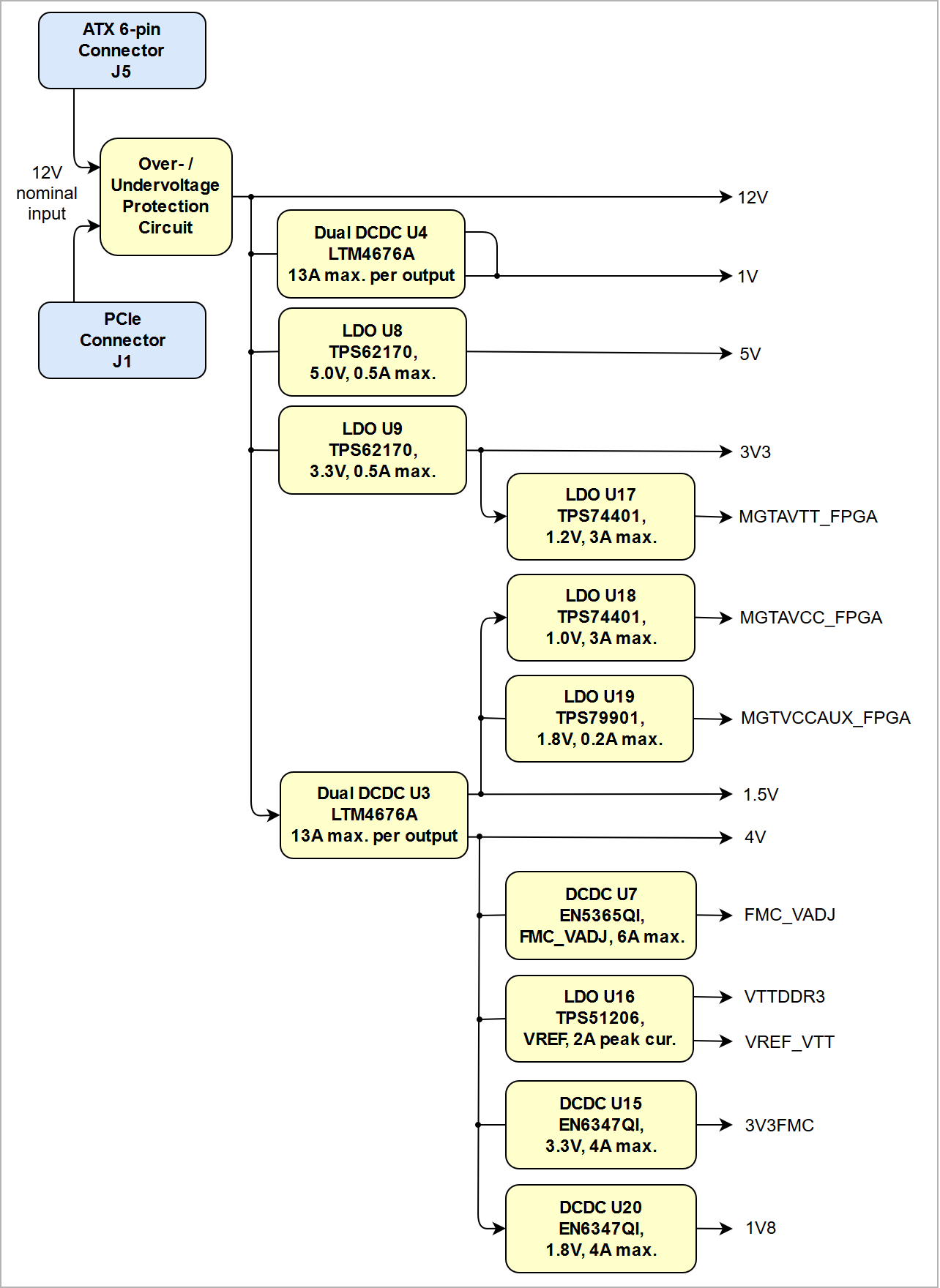
- Xilinx Kintex XC7K-2FBG676I FPGA SoC, U6
- ANSI/VITA 57.1 compliant FMC HPC connector, J2
- Cooling fan 5VDC M1 (45X5MM, 0.7W, 1.06CFM), M1
- PCIe x8 connector, J1
- SODDR3 SODIMM 204-DIMM pin socket, U2
- 6-pin 12V power connector, J5
- Step-down DC-DC converter @1.5V and @4V (LT LTM4676A), U3
- Step-down DC-DC converter @1.0V (LT LTM4676A), U4
- 256 Mbit Quad SPI Flash Memory (Micron N25Q256A), U12
- 10x Green user LEDs connected to FPGA, D1 ... D10
- 4-wire PWM fan connector, J4
- User button, S2
- FPGA JTAG connector, J9
- 4bit DIP switch, S1
- I²C header for LTM4676A DC-DC converter, J10
- System Controller CPLD JTAG header, J8
- 1x Green LED connected to SC CPLD, D11
- 2-pin 5V FAN header, J6
- System Controller CPLD (Lattice Semiconductor LCMXO2-1200HC), U5
- 6A PowerSoC DC-DC converter @FMC_VADJ (Altera EN5365QI), U7
- 4A PowerSoC DC-DC converter @3.3V (3V3FMC) (Altera EN6347QI), U15
- LDO converter @1.2V (MGTAVTT_FPGA) (TI TPS74401RGW), U17
- LDO converter @1.0V (MGTAVCC_FPGA) (TI TPS74401RGW), U18
- 4A PowerSoC DC-DC converter @1.8V (Altera EN6347QI), U7
...
By default the configuration mode pins M[2:0] of the FPGA are set to QSPI mode (Master SPI), hence the FPGA is configured from serial NOR flash QSPI Flash memory at system start-up. The JTAG interface of the module is provided for storing the initial FPGA configuration data to the QSPI flash Flash memory.
Signals, Interfaces and Pins
...
| FPGA Bank | Type | I/O Signal Count | Bank VCCO Voltage | Notes |
|---|---|---|---|---|
| 12 | HR | 48 IO's, 24 LVDS pairs | FMC_VADJ | Bank voltage FMC_VADJ is supplied by DC-DC converter U7 |
| 13 | HR | 34 IO's, 17 LVDS pairs | FMC_VADJ | |
| 15 | HR | 34 IO's, 17 LVDS pairs | FMC_VADJ | |
| 16 | HR | 44 IO's, 22 LVDS pairs | VIO_B_FMC | Bank voltage VIO_B_FMC is supplied by FMC connector J2 |
...
| HTML |
|---|
<!--
TO-DO (future):
If Vivado board part files are available for this module, the standard configuration of the MIO pins by using this board part files should be mentioned here. This standard configuration of those pins are also apparent of the on-board peripherals of base-boards related to the module.
--> |
PCI Express Interface
The TEF1001 FPGA board is a PCI Express card designed to fit into systems with PCI Express x8 slots (PCIe 2.0 or higher) and is PCIe Gen. 2 capable. See next section for the overview of FPGA MGT lanes routed to the PCIe interface.
MGT Lanes
| HTML |
|---|
<!--
MGT lanes should be listed separately, as they are more specific than just general I/Os.
--> |
MGT (Multi Gigabit Transceiver) lane consists of one transmit and one receive (TX/RX) differential pairs, two signals each or four signals total per one MGT lane. The MGT lanes are connected to the FMC connector and to the PCIe x8 connector. Following table lists lane number, MGT bank number, transceiver type, signal schematic name, connector and FPGA pins connection:
...
- PER3_P
- PER3_N
- PET3_P
- PET3_N
...
- J1-A29
- J1-A30
- J1-B27
- J1-B28
...
- MGTXTXP0_115, P2
- MGTXTXN0_115, P1
- MGTXRXP0_115, R4
- MGTXRXN0_115, R3
...
- PER2_P
- PER2_N
- PET2_P
- PET2_N
...
- J1-A25
- J1-A26
- J1-B23
- J1-B24
...
- MGTXTXP1_115, M2
- MGTXTXN1_115, M1
- MGTXRXP1_115, N4
- MGTXRXN1_115, N3
...
- PER1_P
- PER1_N
- PET1_P
- PET1_N
...
- J1-A21
- J1-A22
- J1-B19
- J1-B20
...
- MGTXTXP2_115, K2
- MGTXTXN2_115, K1
- MGTXRXP2_115, L4
- MGTXRXN2_115, L3
...
- PER0_P
- PER0_N
- PET0_P
- PET0_N
...
- J1-A16
- J1-A17
- J1-B14
- J1-B15
...
- MGTXTXP3_115, H2
- MGTXTXN3_115, H1
- MGTXRXP3_115, J4
- MGTXRXN3_115, J3
...
- DP3_M2C_P
- DP3_M2C_N
- DP3_C2M_P
- DP3_C2M_N
...
- J2-A10
- J2-A11
- J2-A30
- J2-A31
...
- MGTXRXP0_116, G4
- MGTXRXN0_116, G3
- MGTXTXP0_116, F2
- MGTXTXN0_116, F1
...
- DP2_M2C_P
- DP2_M2C_N
- DP2_C2M_P
- DP2_C2M_N
...
- J2-A6
- J2-A7
- J2-A26
- J2-A27
...
- MGTXRXP1_116, E4
- MGTXRXN1_116, E3
- MGTXTXP1_116, D2
- MGTXTXN1_116, D1
...
- DP1_M2C_P
- DP1_M2C_N
- DP1_C2M_P
- DP1_C2M_N
...
- J2-A2
- J2-A3
- J2-A22
- J2-A23
...
- MGTXRXP2_116, C4
- MGTXRXN2_116, C3
- MGTXTXP2_116, B2
- MGTXTXN2_116, B1
...
- DP0_M2C_P
- DP0_M2C_N
- DP0_C2M_P
- DP0_C2M_N
...
- J2-C6
- J2-C7
- J2-C2
- J2-C3
...
- MGTXRXP3_116, B6
- MGTXRXN3_116, B5
- MGTXTXP3_116, A4
- MGTXTXN3_116, A3
...
Below are listed MGT banks reference clock sources:
...
Table 4: MGT reference clock sources
JTAG Interface
There are three JTAG interfaces available on the TEF1001 board:
...
CPLD JTAG
VCCIO: 3.3V
Connector: J8
...
J8-4
...
FPGA JTAG
VCCIO: 1.8V
Connector: J9
...
FMC JTAG
VCCIO: 3.3V
Connector: J2
...
Table 5: JTAG interface signals
System Controller CPLD I/O Pins
Special purpose pins are connected to the System Controller CPLD and have following default configuration:
...
JTAG signals between
SC CPLD and FPGA
...
Program FPGA or SC CPLD depending on pin JTAGMODE.
...
PL I/O's are 3-stated until configuration of the FPGA completes.
...
Low active FPGA initialization pin or configuration error signal.
...
 related to the module.
--> |
PCI Express Interface
The TEF1001 FPGA board is a PCI Express card designed to fit into systems with PCI Express x8 slots and has a data transmission capability which meets PCIe Gen. 2. See next section for the overview of FPGA MGT lanes routed to the PCIe interface.
MGT Lanes
| HTML |
|---|
<!--
MGT lanes should be listed separately, as they are more specific than just general I/Os.
--> |
MGT (Multi Gigabit Transceiver) lane consists of one transmit and one receive (TX/RX) differential pairs, two signals each or four signals total per one MGT lane. The MGT lanes are connected to the FMC connector and to the PCIe x8 connector. Following table lists lane number, MGT bank number, transceiver type, signal schematic name, connector and FPGA pins connection:
| Lane | Bank | Type | Signal Name | PCIe Connector Pin | FPGA Pin |
|---|---|---|---|---|---|
| 0 | 115 | GTX |
|
|
|
| 1 | 115 | GTX |
|
|
|
| 2 | 115 | GTX |
|
|
|
| 3 | 115 | GTX |
|
|
|
| Lane | Bank | Type | Signal Name | FMC Connector Pin | FPGA Pin |
| 0 | 116 | GTX |
|
|
|
| 1 | 116 | GTX |
|
|
|
| 2 | 116 | GTX |
|
|
|
| 3 | 116 | GTX |
|
|
|
Table 3: FPGA to B2B connectors routed MGT lanes overview
Below are listed MGT banks reference clock sources:
| Clock signal | Bank | Source | FPGA Pin | Notes |
|---|---|---|---|---|
| MGTCLK_5338_P | 115 | U13, CLK1A | MGTREFCLK0P_115, H6 | Supplied by on-board Si5338A |
| MGTCLK_5338_N | U13, CLK1B | MGTREFCLK0N_115, H5 | ||
| PCIE_CLK_P | 115 | J1-A13, REFCLK+ | MGTREFCLK1P_115, K6 | External clock from PCIe slot |
| PCIE_CLK_N | J1-A14, REFCLK- | MGTREFCLK1N_115, K6 | ||
| GBTCLK0_M2C_P | 116 | J2-D4 | MGTREFCLK0P_116, D6 | External clock from FMC connector |
| GBTCLK0_M2C_N | J2-D5 | MGTREFCLK0N_116, D5 | ||
| GBTCLK1_M2C_P | 116 | J2-B20 | MGTREFCLK1P_116, F6 | External clock from FMC connector |
| GBTCLK1_M2C_N | J2-B21 | MGTREFCLK1N_116, F5 |
Table 4: MGT reference clock sources
JTAG Interface
There are three JTAG interfaces available on the TEF1001 board:
| JTAG Interface | Signal Schematic Name | JTAG Connector Pin | Connected to |
|---|---|---|---|
CPLD JTAG VCCIO: 3.3V Connector: J8 | CPLD_JTAG_TMS | J8-1 | SC CPLD, bank 0, pin 90 |
| CPLD_JTAG_TDI | J8-2 | SC CPLD, bank 0, pin 94 | |
| CPLD_JTAG_TDO | J8-3 | SC CPLD, bank 0, pin 95 | |
| CPLD_JTAG_TCK | J8-4 | SC CPLD, bank 0, pin 91 | |
FPGA JTAG VCCIO: 1.8V Connector: J9 | FPGA_JTAG_TMS | J9-4 | FPGA, bank 0, pin N9 |
| FPGA_JTAG_TCK | J9-6 | FPGA, bank 0, pin M8 | |
| FPGA_JTAG_TDO | J9-8 | FPGA, bank 0, pin N8 | |
| FPGA_JTAG_TDI | J9-10 | FPGA, bank 0, pin L8 | |
FMC JTAG VCCIO: 3.3V Connector: J2 | FMC_TRST | J2-D34 | SC CPLD, bank 2, pin 36 |
| FMC_TCK | J2-D29 | SC CPLD, bank 2, pin 27 | |
| FMC_TMS | J2-D33 | SC CPLD, bank 2, pin 28 | |
| FMC_TDI | J2-D30 | SC CPLD, bank 2, pin 31 | |
| FMC_TDO | J2-D31 | SC CPLD, bank 2, pin 32 |
Table 5: JTAG interface signals
System Controller CPLD I/O Pins
Special purpose pins are connected to the System Controller CPLD and have following default configuration:
| Pin Name | SC CPLD Direction | Function | Default Configuration |
|---|---|---|---|
| 200MHZCLK_EN | out | control line | enables 200.0000MHz oscillator U1 |
| BUTTON | in | user | Reset Button |
| CPLD_TDO | out | CPLD JTAG interface | - |
| CPLD_TDI | in | ||
| CPLD_TCK | in | ||
| CPLD_TMS | in | ||
| DDR3_SCL | in / out | I²C data line | I²C bus of DDR3 SODIMM socket |
| DDR3_SDA | in / out | I²C clock | |
| FEX_DIR / FEX0 ... FEX11 | in / out | user GPIO | see current SC CPLD firmware |
| F1PWM | out | FAN control | see current SC CPLD firmware |
| F1SENSE | in | see current SC CPLD firmware | |
| FMC_PG_C2M | out | FMC signals and pins | see current SC CPLD firmware |
| FMC_PG_M2C | in | ||
| FMC_PRSNT_M2C_L | in | ||
| FMC_SCL | in / out | FMC I²C | I²C connected to FPGA |
| FMC_SDA | in / out | ||
| FMC_TCK | FMC JTAG | see current SC CPLD firmware | |
| FMC_TDI | |||
| FMC_TDO | |||
| FMC_TMS | |||
| FMC_TRST | |||
| DONE | in | FPGA config signal | PL configuration completed |
| PROGRAM_B | out | PL configuration reset signal | |
| LED1 ... LED2 | out | LED status signal | see current CPLD firmware |
| FPGA_IIC_OE | in | FPGA I²C | I²C operation enable |
| FPGA_IIC_SCL | out | I²C clock line | |
| FPGA_IIC_SDA | out | I²C data line | |
| EN_1V | out | Power control | enable signal DCDC U13 '1V' |
| PG_1V | in | power good signal DCDC U13 '1V' | |
| EN_1.0V_MGT | out | enable signal DCDC U16 '1.0V_MGT' | |
| PG_1.0V_MGT | in | power good signal DCDC U16 '1.0V_MGT' | |
| EN_1.2V_MGT | out | enable signal DCDC U16 '1.2V_MGT' | |
| PG_1.2V_MGT | in | power good DCDC U16 '1.2V_MGT' | |
| EN_1.8V | out | enable signal DCDC U16 '1.8V' | |
| PG_1.8V | in | power good signal DCDC U16 '1.8V' | |
| EN_3.3V | out | enable signal DCDC U16 '3.3V' | |
| PG_3.3V | in | power good signal DCDC U16 '3.3V' | |
| PG_1V5 | in | power good signal DCDC U23 '1.5V' |
Table 6: System Controller CPLD I/O pins
Table 6: System Controller CPLD I/O pins
...
- FPGA_IIC_SDA, pin 24
- FPGA_IIC_SCL, pin 25
- FPGA_IIC_OE, pin 19
...
- FPGA bank 16, pin V29
- FPGA bank 16, pin W29
- FPGA bank 16, pin W26
...
VCCIO: 1V8, all with pull-up to 1V8.
Following devices and connectors are linked to the FPGA_IIC I2C interface:
- DC-DC converter U3 and U4 (LT LTM4676)
- Programmable quad clock generator U13
- FMC connector J2
- PCIe connector J1
Note: FPGA_IIC_OE must kept high for I2C operation.
For I2C slave device addresses refer to the component datasheets.
...
User I/Os
External LVDS pairs
...
10 I/Os
5 x LVDS pairs
...
- EX0_P ... EX4_P
- EX0_N ... EX4_N
...
- IDC header J7
...
Can also be used for single-ended signaling.
...
User I/Os
Internal LVDS pairs
...
13 I/Os
6 x LVDS pairs
...
- FEX0_P ... FEX5_P
- FEX0_N ... FEX5_N
- FEX_DIR (single-ended I/O)
...
- FPGA bank 18
...
VCCIO: 1V8
Can also be used for single-ended signaling.
FPGA bank 18 has also reference clock input from FMC connector (CLK2, CLK3) and clock synthesizer U9 (FCLK).
Internal signal assignment:
FEX_DIR <= FMC_PRSNT_M2C_L
...
- DONE, pin 7
- PROGRAM_B, pin 8
...
- FPGA bank 0, pin V8
- FPGA bank 0, pin U8
...
- PLL_SCL, pin 14
- PLL_SDA, pin 15
...
- U13, pin 12
- U13, pin 19
...
VCCIO: 1V8
Only PLL_SDA has 1V8 pull-up.
...
- F1SENSE, pin 99
- F1PWM, pin 98
...
- J4-3 (active low)
- J4-4
...
Internal signal assignment:
- FEX_5_P <= F1SENSE
- FEX_5_N => F1PWM
...
- BUTTON, pin 77
...
- Switch S2
...
- LED1, pin 76
...
- LED D1 (green)
...
Fast blinking, when FPGA is not programmed.
Internal signal assignment:
- LED1 <= Button S2 or FEX0_P
...
PCIe control line RESET_B
...
- PCIE_RSTB, pin 37
...
- J1-A11
...
Internal signal assignment:
- FEX_4_N <= PCIE_RSTB
...
Control interface to clock synthesizer U9 (TI LMK04828B)
...
SPI (3 I/Os),
4 I/Os
...
- CLK_SYNTH_SDIO, pin 75
- CLK_SYNTH_SCK, pin 74
- CLK_SYNTH_RESET, pin 54
- CLK_SYNTH_CS, pin 53
- CLK_SYNTH_SYNC, pin 52
- LMK_STAT0, pin 62
- LMK_STAT1, pin 63
...
- U9, pin 20
- U9, pin 19
- U9, pin 5
- U9, pin 18
- U9, pin 6
- U9, pin 31
- U9, pin 48
...
Pull up to 3V3PCI.
- Internal signal assignment:
- LMK_SCK <= FEX_1_P
- LMK_SDIO <= FEX_1_N
- LMK_CS <= FEX_3_P
- LMK_SYNC <= EX_3_N
- LMK_RESET <= FEX_4_P
- FEX_2_P => LMK_SDIO (FEX_2_N must be 0)
- LMK_STAT0 and LMK_STAT1 signals are not used.
...
I2C (2 I/Os),
2 I/Os
...
- LTM_SCL, pin 67
- LTM_SDA, pin 66
- LTM1_ALERT, pin 65
- LTM2_ALERT, pin 64
...
- U4, pin E6 and U3, pin E6
- U4, pin D6 and U3, pin D6
- U4, pin E5
- U3, pin E5
...
3V3 pull-ups.
LTM I2C interface is also accessible trough header J10.
LTM1_ALERT and LTM2_ALERT signals are not used.
...
- EN_1V8, pin 58
- PG_1V8, pin 59
- EN_FMC_VADJ, pin 60
- PG_FMC_VADJ, pin 61
- EN_3V3, pin 51
- PG_3V3, pin 57
...
- U20, pin 27
- U20, pin 28
- U7, pin 27
- U7, pin 28
- U15, pin 27
- U15, pin 28
...
Sequence of the supply voltages depend on the System Controller CPLD firmware.
EN_1V8, EN_3V3 and EN_FMC_VADJ will be set simultaneously at start-up.
PG signals will not be evaluated.
For detailed function of the pins and signals, the internal signal assignment and the implemented logic, look to the Wiki reference page of the module's SC CPLD or into its bitstream file.
...
| Scroll Title | ||||||||||||||||||||||||||||||||
|---|---|---|---|---|---|---|---|---|---|---|---|---|---|---|---|---|---|---|---|---|---|---|---|---|---|---|---|---|---|---|---|---|
| ||||||||||||||||||||||||||||||||
|
...
|
Power-On Sequence
The TE0841 SoM meets the recommended criteria to power up the Xilinx FPGA properly by keeping a specific sequence of enabling the on-board DC-DC converters dedicated to the particular functional units of the FPGA chip and powering up the on-board voltages.
...
| HTML |
|---|
<!--
Set correct link to the overview table of the product on english and german, if not available, set
https://shop.trenz-electronic.de/de/Produkte/Trenz-Electronic/
https://shop.trenz-electronic.de/en/Products/Trenz-Electronic/
--> |
...
Absolute Maximum Ratings
Parameter | Min | Max | Units | Reference Document | ||
|---|---|---|---|---|---|---|
VIN supply voltage | -0.3 | 6.020 | V | EN63A0QI, TPS74401RGW datasheets | ||
| 3.3VIN supply voltage | -0.1 | 3.4 | V | Xilinx datasheet DS892 (HR Bank VCCO) | ||
TPS6217 datasheet Caution with FMC module plugged in: VIN range 11.4V ... 12.6V | VBAT_IN | -0.3 | 6.0 | V | TPS780xx datasheet | |
| Supply voltage for HR I/O banks (VCCO) | -0.500 | 3. | 400600 | V | Xilinx datasheet DS182 | |
Supply voltage for HP I/O banks (VCCO) | -0.500 | 2.000 | V | Xilinx datasheet DS892datasheet DS182 | ||
| I/O input voltage for HR I/O banks | -0. | 400500 | VCCO + 0. | 550500 | V | Xilinx datasheet DS892DS182 |
I/O input voltage for HP I/O banks | -0. | 550500 | VCCO + 0. | 550500 | V | Xilinx datasheet DS182 |
| Reference Voltage pin (VREF) | -0.500 | 2 | V | Xilinx datasheet DS182 | ||
| Differential input voltage | -0.5 | 2.625 | V | Xilinx datasheet DS892datasheet DS182 | ||
| I/O input voltage for SC CPLD U18U5 | -0.5 | 3.75 | V | LCMXO2-256HC Lattice MachXO2 Family datasheet | ||
| GTH and GTY transceiver reference clocks absolute input voltage (MGT_CLK0, MGT_CLK2) | -0.500 | 1.320 | V | Xilinx datasheet DS892datasheet DS182 | ||
GTH and GTY transceiver receiver (RXP/RXN) and transmitter (TXP/TXN) absolute input voltageTXP/TXN) absolute input voltage | -0.500 | 1.260 | V | Xilinx datasheet DS182 | ||
| Voltages on LTM4676 I²C pins (LTM_SCL, LTM_SDA), header J10 | -0. | 5003 | 15. | 2605 | V | Xilinx LTM4676A datasheet DS892 |
Storage temperature | -40 | +100 | °C | SML-P11 LED datasheet |
Table 16: Module absolute maximum ratings
...
Recommended Operating Conditions
| Parameter | Min | Max | Units | Reference Document | ||
|---|---|---|---|---|---|---|
| VIN supply voltage3 | 11. | 34 | 512. | 56 | V | TPS82085SIL, TPS74401RGW datasheet |
| 3.3VIN supply voltage | 3.3 | 3.4 | V | Xilinx datasheet DS892 (HR Bank VCCO) | ||
| VBAT_IN | 2.2 | 5.5 | V | TPS780xx datasheet | ||
| 12V nominal, ANSI/VITA 57.1 power specification for FMC connector | ||||||
| Supply voltage for HR I/O banks (VCCO) | 1.140 | 3. | 400465 | V | Xilinx datasheet DS892datasheet DS182 | |
Supply voltage for HP I/O banks (VCCO)0 | 1. | 950140 | 1.890 | V | Xilinx datasheet DS892datasheet DS182 | |
I/O input voltage for HR I/O banks | –0. | 200500 | VCCO + 0.20 | V | Xilinx datasheet DS892datasheet DS182 | |
| I/O input voltage for HP I/O banks | –0. | 200500 | VCCO + 0.20 | V | Xilinx datasheet DS182 | |
| Differential input voltage | -0.2 | 2.625 | V | Xilinx datasheet DS182 datasheet DS892 | ||
| I/O input voltage for SC CPLD U18U5 | -0.3 | 3.6 | V | Lattice MachXO2 Family datasheet | ||
| Voltages on LTM4676 I²C pins (LTM_SCL, LTM_SDA), header J10 | 0 | 3.3V | V | LCMXO2-256HC LTM4676A datasheet | ||
Industrial Module Operating Temperature Range | -40 | 85 | °C | Xilinx datasheet DS892datasheet DS182 | ||
| Commercial Module Operating Temperature Range | 0 | 85 | °C | Xilinx DS892DS182, Silicon Labs Si5338 datasheet |
...
| Date | Revision | Notes | PCN | Documentation Link | ||
|---|---|---|---|---|---|---|
| 2018-05-11 | 02 | current available board revisionPCN | - | 20180511TE0841 | - | 02|
| 2015-12-09 | 01 | First production release | PCN-20180524 TEF1001-01TE0841 | TEF1001-01 |
Table 18: Module hardware revision history
...
| Scroll Title | ||||
|---|---|---|---|---|
| ||||
|
Document Change History
| HTML |
|---|
<!-- Generate new entry: 1.add new row below first 2.Copy "Page Information Macro(date)" Macro-Preview, Metadata Version number, Author Name and description to the empty row. Important Revision number must be the same as the Wiki document revision number 3.Update Metadata = "Page Information Macro (current-version)" Preview+1 and add Author and change description. --> |
Date | Revision | Contributors | Description | ||||||||||||||||||||||||||
|---|---|---|---|---|---|---|---|---|---|---|---|---|---|---|---|---|---|---|---|---|---|---|---|---|---|---|---|---|---|
|
|
|
|
Table 18: Document change history
...
Overview
Content Tools