...
Special purpose pins are connected to the System Controller CPLD and have following default configuration:
| Pin Name | SC CPLD Direction | Function | Default Configuration |
|---|
| 200MHZCLK_EN | out | control line | enables 200.0000MHz oscillator U1 |
| BUTTON | in | user | Reset Button |
| CPLD_TDO | out | CPLD JTAG interface
| - |
| CPLD_TDI | in |
| CPLD_TCK | in |
| CPLD_TMS | in |
| JTAG_EN | in |
| DDR3_SCL | in / out | I²C |
data lineI²C bus of DDR3 SODIMM socket
| I²C connected to FPGA |
| DDR3_SDA | in / out |
| PLL_SCL | in / out | I²C bus of SI5338 quad clock PLL | I²C connected to FPGA |
| PLL_SDA | in / out |
| PCIE_RSTB | in | PCIe reset input | see current SC CPLD firmware |
| FEX_DIR / FEX0 ... FEX11 | in / out | user GPIO | see current SC CPLD firmware |
| F1PWM | out | FPGA FAN control | see current SC CPLD firmware |
| F1SENSE | in |
see current SC CPLD firmware| FAN_FMC_EN | out | FMC FAN enable |
| FMC_PG_C2M | out | FMC signals and pins | see current SC CPLD firmware |
| FMC_PG_M2C | in |
| FMC_PRSNT_M2C_L | in |
| FMC_SCL | in / out | FMC I²C | I²C connected to FPGA |
| FMC_SDA | in / out |
| FMC_TCK |
| FMC JTAG | see current SC CPLD firmware |
| FMC_TDI |
|
| FMC_TDO |
|
| FMC_TMS |
|
| FMC_TRST |
|
| DONE | in | FPGA |
config | configuration signal | PL configuration completed |
| PROGRAM_B | out | PL configuration reset signal |
| LED1 |
... LED2 | out | LED status signal | see current CPLD firmware |
| FPGA_IIC_OE | in | FPGA I²C | I²C operation enable |
| FPGA_IIC_SCL | in / out | I²C clock line |
| FPGA_IIC_SDA | in / out | I²C data line |
| EN_ |
1V| 1V8 | out | Power control | enable signal DCDC |
U13 1V1V| 1V8 | in | power good signal DCDC |
U13 1V1.0V_MGT| 3V3FMC | out | enable signal DCDC |
U16 1.0VMGT1.0V_MGT DCDC U16 '1.0V_MGT1.2VMGT| VADJ | out | enable signal DCDC |
U16 1.2VMGT1.2VMGT U16 1.2VMGT| EN_1.8V | out | enable signal DCDC U16 '1.8V' |
| PG_1.8V | in | power good signal DCDC U16 '1.8V' |
| EN_3.3V | out | enable signal DCDC U16 '3.3V' |
| PG_3.3V | in | power good signal DCDC U16 '3.3V' |
| PG_1V5 | in | power good signal DCDC U23 '1.5V' |
VID0_FMC_VADJ,
VID1_FMC_VADJ,
VID2_FMC_VADJ | out | DCDC U7 power selection pin |
VID0_FMC_VADJ_CTRL,
VID1_FMC_VADJ_CTRL,
VID2_FMC_VADJ_CTRL | in | Power selection of FMC_VADJ, forwarded
to DCDC U7 |
| LTM_1V5_RUN | out | enable signals of DCDC U3, U4 (LTM4676)
see current CPLD firmware |
| LTM_4V_RUN | out |
| LTM_SCL | in / out | DCDC U3, U4 (LTM4676) I²C | I²C connected to FPGA |
| LTM_SDA | in / out |
| LTM1_ALERT | in | DCDC U3, U4 (LTM4676) control | see current CPLD firmware |
| LTM2_ALERT | in |
| LTM_1V_IO0 | in / out |
| LTM_1V_IO1 | in / out |
| LTM_1V5_4V_IO0 | in / out |
| LTM_1V5_4V_IO1 | in / out |
Table 6: System Controller CPLD I/O pins
...
Quad SPI interface is connected to the FPGA configuration FPGA bank 14, QSPI clock is provided by FPGA config bank 0.
| Signal Name | QSPI Flash Memory U6 U12 Pin | FPGA Pin |
|---|
| SPIFLASH_QSPI_CS | C2 | RDWR_FCS_B_0, AH7 |
| SPIFLASH_QSPI_D0 | D3 | D00_MOSI_0, AA7 |
| SPIFLASH_QSPI_D1 | D2 | D01_DIN_0, Y7 |
| SPIFLASH_QSPI_D2 | C4 | D02_0, U7 |
| SPIFLASH_QSPI_D3 | D4 | D03_0, V7 |
| SPIFLASH_CFG_CLKCCLK | B2 | CCLK_0, V11 |
Table 7: Quad SPI interface signals and connections
...
For detailed information, refer to the reference page of the SC CPLD firmware of this module.
...
| Scroll Title |
|---|
| anchor | Figure_4 |
|---|
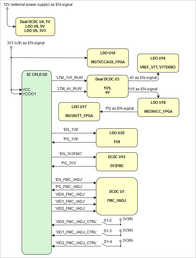
| title | Figure 4: TEF1001-02 Power-On Sequence Diagram |
|---|
|
| Scroll Ignore |
|---|
| draw.io Diagram |
|---|
| border | false |
|---|
| viewerToolbar | true |
|---|
| |
|---|
| fitWindow | false |
|---|
| diagramDisplayName | |
|---|
| lbox | true |
|---|
| revision | 34 |
|---|
| diagramName | TEF1001 power-on sequence diagram |
|---|
| simpleViewer | false |
|---|
| width | |
|---|
| links | auto |
|---|
| tbstyle | hidden |
|---|
| diagramWidth | 642 |
|---|
|
|
| Scroll Only |
|---|
|
|
...