...
| Scroll Title |
|---|
| anchor | Table_x |
|---|
| title | Table x: Typical power consumption. |
|---|
|
| Scroll Table Layout |
|---|
| orientation | portrait |
|---|
| sortDirection | ASC |
|---|
| repeatTableHeaders | default |
|---|
| style | |
|---|
| widths | |
|---|
| sortByColumn | 1 |
|---|
| sortEnabled | false |
|---|
| cellHighlighting | true |
|---|
|
| Power Input | Typical Current |
|---|
| VIN_12V | TBD* |
|
Power
...
| anchor | Figure_3 |
|---|
| title | Figure 3: Power Distribution |
|---|
supply with minimum current capability of 6.65A for system startup is recommended.
The TEC0850 board is equipped with the Xilinx Zynq UltraScale+ MPSoC delivers a heterogeneous multi-processing system with integrated programmable logic and independently operable elements and is designed to meet embedded system power management requirement by advanced power management features. This features allow to offset the power and heat constraints against overall performance and operational efficiency.
This features allowing highly flexible power management are achieved by establishing Power Domains for power isolation. The Zynq UltraScale+ MPSoC has multiple power domains, whereby each power domain requires its own particular on-board DC-DC converters.
The Processing System contains three Power Domains:
- Battery Power Domain (BBRAM and RTC)
- Full-Power Domain (Application Processing Unit, DDR Controller, Graphics Processing Unit and High-Speed Connectivity)
- Low-Power Domain (Real-Time Processing Unit, Security and Configuration Unit, Platform Management Unit, System Monitor and General Connectivity)
- Programmable Logic (PL)
Power Distribution Dependencies
There are following dependencies how the initial 24V voltage from the main power pins on cPCI slot J1 is distributed to the on-board DC-DC converters, which power up further DC-DC converters and the particular on-board voltages:
| Scroll Title |
|---|
| anchor | Figure_3 |
|---|
| title | Figure 3: Power Distribution |
|---|
|
| Scroll Ignore |
|---|
| draw.io Diagram |
|---|
| border | false |
|---|
| viewerToolbar | true |
|---|
| |
|---|
| fitWindow | false |
|---|
| diagramDisplayName | |
|---|
| lbox | true |
|---|
| revision | 16 |
|---|
| diagramName | Power supply |
|---|
| simpleViewer | true |
|---|
| width | |
|---|
| links | auto |
|---|
| tbstyle | hidden |
|---|
| diagramWidth | 641 |
|---|
|
|
| Scroll Only |
|---|
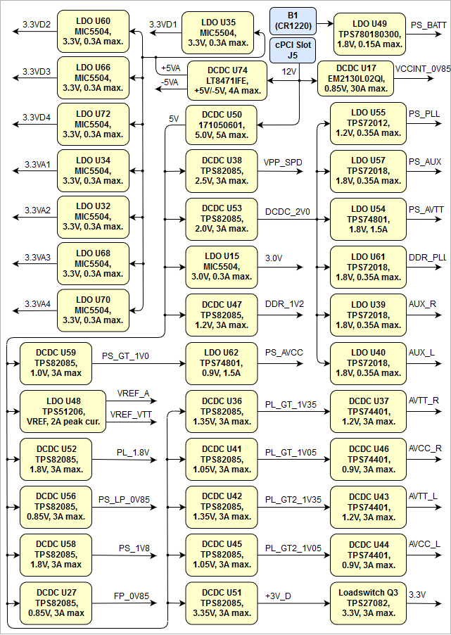 Image Added Image Added
|
|
Power-On Sequence
The TEC0850 board meets the recommended criteria to power up the Xilinx Zynq UltraScale+ MPSoC properly by keeping a specific sequence of enabling the on-board DC-DC converters dedicated to the particular Power Domains and powering up the on-board voltages.
On the TEB0911 UltraRack board following Power Domains will be powered up in a certain sequence with by enable and power-good signals of the DC-DC converters, which are controlled by the System Controller FPGA U18:
- Low-Power Domain (LPD)
- Programmable Logic (PL) and Full-Power Domain (FPD)
- GTH, PS GTR transceiver and DDR memory
Hence, those three power instances will be powered up consecutively when the Power-Good signals of the previous instance is asserted.
Following diagram describes the sequence of enabling the three power instances utilizing the DC-DC converter control signals (Enable, Power-Good), which will power-up in descending order as listed in the blocks of the diagram.
...
| Scroll Only |
|---|
Image Removed |
...
| Scroll Title |
|---|
| anchor | Figure_4 |
|---|
| title | Figure 4: Power-On Sequence Diagram |
|---|
|
| Scroll Ignore |
|---|
| draw.io Diagram |
|---|
| border | false |
|---|
| viewerToolbar | true |
|---|
| fitWindow | false |
|---|
diagramDisplayName | | lbox | true |
|---|
| revision | 2 |
|---|
| diagramName | TEC0850 Power-On Sequence Diagram |
|---|
| simpleViewer | false |
|---|
width | | links | auto |
|---|
| tbstyle | hidden |
|---|
| diagramWidth | 641 |
|---|
|
|
| Scroll Only |
|---|
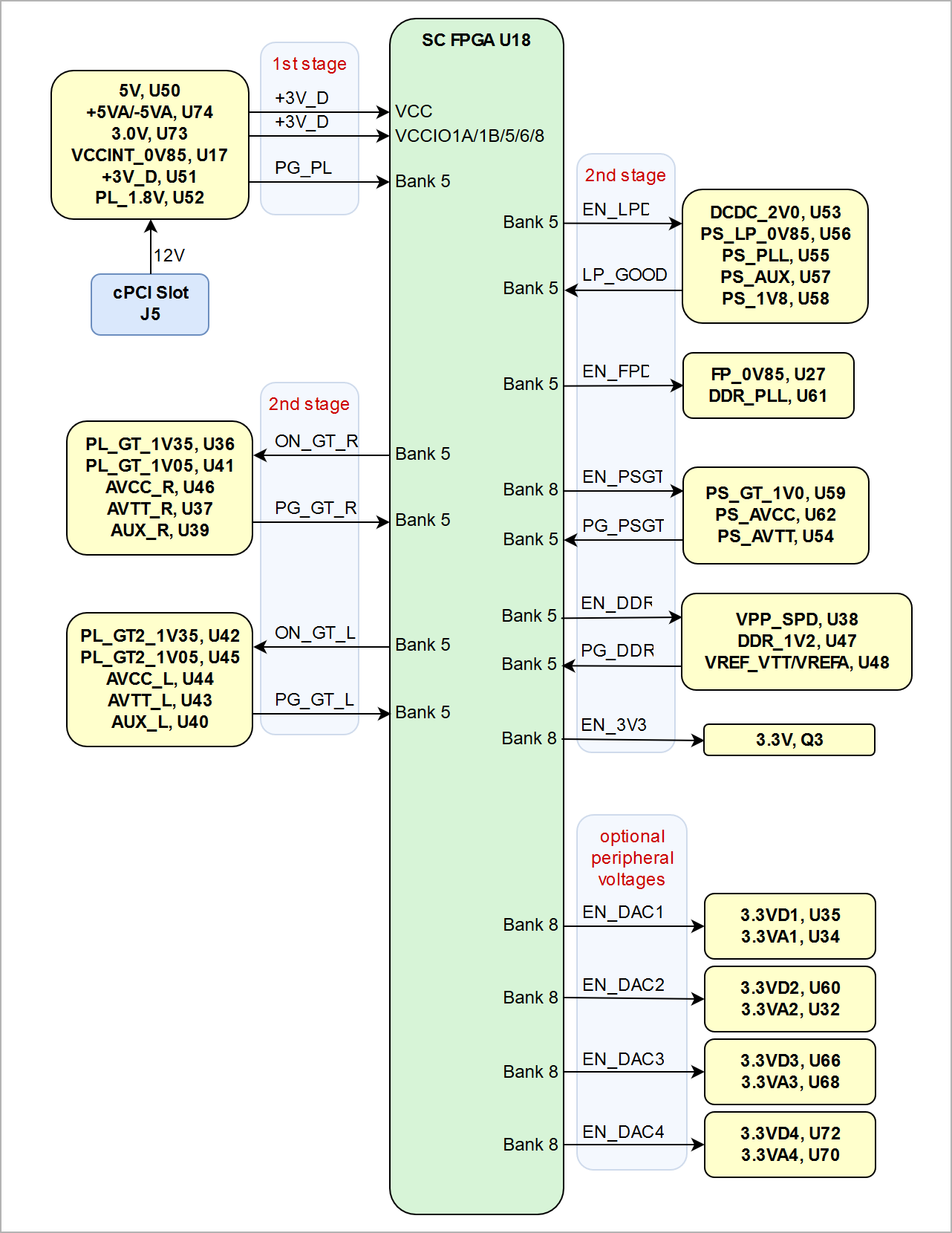 Image Removed Image Removed
|
|
...
| false | | viewerToolbar | true |
|---|
| |
|---|
| fitWindow | false |
|---|
| diagramDisplayName | |
|---|
| lbox | true |
|---|
| revision | 2 |
|---|
| diagramName | TEC0850 Power-On Sequence Diagram |
|---|
| simpleViewer | false |
|---|
| width | |
|---|
| links | auto |
|---|
| tbstyle | hidden |
|---|
| diagramWidth | 641 |
|---|
|
|
| Scroll Only |
|---|
Image Added |
|
| Warning |
|---|
| To avoid any damage to the MPSoC module, check for stabilized on-board voltages in steady state before powering up the MPSoC's I/O bank voltages VCCOx. All I/Os should be tri-stated during power-on sequence. |
It is important that all PS and PL I/Os are tri-stated at power-on until the "Power Good"-signals are high, meaning that all on-board voltages have become stable and module is properly powered up.
See Xilinx datasheet DS925 for additional information.
Voltage Monitor Circuit
The voltages PS_1V8 and VCCINT_0V85 are monitored by the voltage monitor circuit U69, which generates the POR_B reset signal at power-on. A manual reset is also possible by driving the low active MR-pin connected to MAX10 FPGA U18 (bank5, pin K10) to GND.
| Scroll Title |
|---|
| anchor | Figure_4 |
|---|
| title | Figure 4: Power-On Sequence Diagram |
|---|
|
| Scroll Ignore |
|---|
| draw.io Diagram |
|---|
| border | truefalse |
|---|
| viewerToolbar | true |
|---|
| |
|---|
| fitWindow | false |
|---|
| diagramDisplayName | |
|---|
| lbox | true |
|---|
| revision | 1 |
|---|
| diagramName | TEC0850 Voltage Monitor Circuit |
|---|
| simpleViewer | false |
|---|
| width | |
|---|
| links | auto |
|---|
| tbstyle | hidden |
|---|
| diagramWidth | 642 |
|---|
| revision | 1 |
|---|
|
|
| Scroll Only |
|---|
 Image Added Image Added
|
|
Power Rails
| Scroll Title |
|---|
| anchor | Table_x |
|---|
| title | Table x: Module absolute maximum ratings. |
|---|
|
| Scroll Table Layout |
|---|
| orientation | portrait |
|---|
| sortDirection | ASC |
|---|
| repeatTableHeaders | default |
|---|
| style | |
|---|
| widths | |
|---|
| sortByColumn | 1 |
|---|
| sortEnabled | false |
|---|
| cellHighlighting | true |
|---|
|
| Connector / Pin | Voltage | Direction | Notes |
|---|
| J1, pin A1, D1, E1, G1, H1, J1, K1 | VIN_12V | Input | Main power supply pins | | J17, pin 2 | 12V | Output | 4-wire PWM fan connector supply voltage | | J13, pin 4 | +3V_D | Output | JTAG/UART reference VCCIO voltage | | B1, pin + | VBATT | Input | 3.0V CR1220 battery | | J16, pin 2 | 5V | Output | I/O header VCCIO | | J16, pin 1 | 3.3V | Output | I/O header VCCIO | | J9, pin 4 | VBUS | Input | USB2 VBUS (5.0V nominal) | | J10, pin A4, B9 | VBUS30 | Input | USB3 VBUS (5.0V nominal) | | J11, pin 4 | 3.3V | Output | MicroSD Card VDD | | J15, pin 2 | DAC1_OUT | Output | DAC output | | J15, pin 3 | DAC2_OUT | Output | DAC output | | J15, pin 4 | DAC3_OUT | Output | DAC output | | J15, pin 5 | DAC4_OUT | Output | DAC output |
|
Bank Voltages
| Scroll Title |
|---|
| anchor | Table_x |
|---|
| title | Table x: Module absolute maximum ratings. |
|---|
|
| Scroll Table Layout |
|---|
| orientation | portrait |
|---|
| sortDirection | ASC |
|---|
| repeatTableHeaders | default |
|---|
| style | |
|---|
| widths | |
|---|
| sortByColumn | 1 |
|---|
| sortEnabled | false |
|---|
| cellHighlighting | true |
|---|
|
| Zynq MPSoC Bank | Type | Schematic Name | Voltage | Voltage Range |
|---|
| 44 | HD | 3.3V | 3.3V | fixed to 3.3V | | 47 | HD | 3.3V | 3.3V | fixed to 3.3V | | 48 | HD | 3.3V | 3.3V | fixed to 3.3V | | 49 | HD | 3.3V | 3.3V | fixed to 3.3V | | 50 | HD | 3.3V | 3.3V | fixed to 3.3V | | 64 | HP | PL_1V8 | 1.8V | fixed to 1.8V | | 65 | HP | PL_1V8 | 1.8V | fixed to 1.8V | | 66 | HP | PL_1V8 | 1.8V | fixed to 1.8V | | 67 | HP | PL_1V8 | 1.8V | fixed to 1.8V | | 500 | MIO | PS_1V8 | 1.8V | fixed to 1.8V | | 501 | MIO | PS_1V8 | 1.8V | fixed to 1.8V | | 502 | MIO | PS_1V8 | 1.8V | fixed to 1.8V | | 503 | CONFIG | PS_1V8 | 1.8V | fixed to 1.8V | | 504 | PSDDR | DDR_1V2
DDR_PLL | 1.2V
1.8V | fixed bank voltages | 128 129 130 | GTH | AVCC_L AUX_L AVTT_L | 0.9V 1.8V 1.2V | fixed bank voltages | 228 229 230 | GTH | AVCC_R AUX_R AVTT_R | 0.9V 1.8V 1.2V | fixed bank voltages | | MAX10 FPGA Bank | Type | Schematic Name | Voltage | Voltage Range |
|---|
| 1A | - | +3V_D | 3.3V | fixed to 3.3V | | 1B | - | +3V_D | 3.3V | fixed to 3.3V | | 2 | - | PS_1V8 | 1.8V | fixed to 1.8V | | 3 | - | 3.3V | 3.3V | fixed to 3.3V | | 5 | - | +3V_D | 3.3V | fixed to 3.3V | | 6 | - | +3V_D | 3.3V | fixed to 3.3V | | 8 | - | +3V_D | 3.3V | fixed to 3.3V |
|
Technical Specifications
Absolute Maximum Ratings
...