...
Zynq UltraScale+ MPSoC ZU15
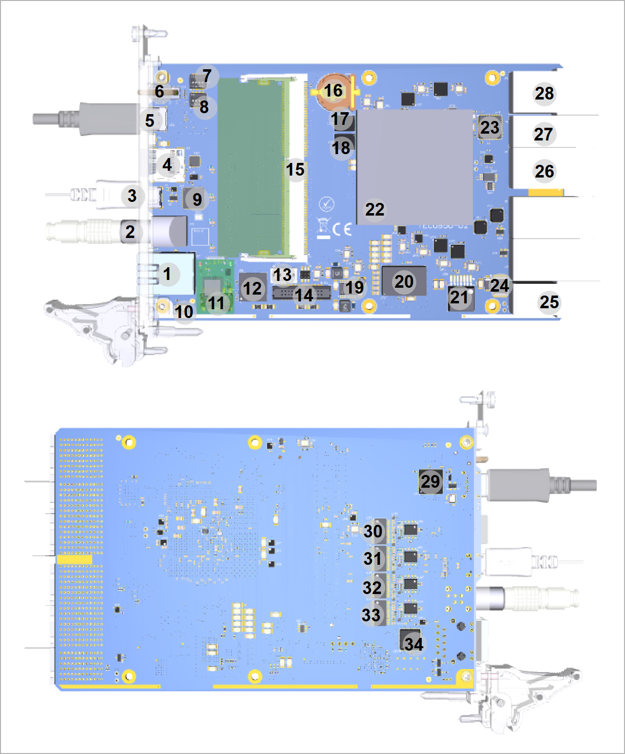
- Front side interface connectors
- RJ-45 GbE Ethernet interface
- Elbow Socket Circular push/pull connector with 4x on-board 8bit DAC output
- MicroSD Card connector
- USB2 and USB3 to FIFO bridge connector
- 4x status LEDs
- 4 CompactPCI connectors for backplane connection (3U form factor)
- 24 GTH lanes
- 4 PS GTR lanes
- USB2 interface
- 64 Zynq PL HP I/O's
- 8x PLL clock input
- JTAG, I²C and 7 user I/O's to MAX10 FPGA
64bit DDR4 SODIMM (PS connected), 8 GByte maximum
Dual parallel QSPI Flash (bootable), 512 MByte maximum
- 26-pin header with 20 Zynq PL HD I/O's
- 3-pin header with 2 MAX10 FPGA I/O's
- System Controller (Altera MAX10 FPGA SoC)
- Power Sequencing
- System management and control for MPSoC and on-board peripherals
- Si5345 programmable 10 output PLL clock generator
- Si53340 Quad PLL clock generatorbuffer
- 2x 4bit DIP switches
- 1x user push button
- Zynq MPSoC cooling FAN connector
- On-board high-efficiency DC-DC converters
...
| Scroll Title |
|---|
| anchor | Figure_2 |
|---|
| title | Figure 2: TEC0850-02 main components |
|---|
|
| Scroll Ignore |
|---|
| draw.io Diagram |
|---|
| border | false |
|---|
| viewerToolbar | true |
|---|
| |
|---|
| fitWindow | false |
|---|
| diagramDisplayName | |
|---|
| lbox | true |
|---|
| revision | 5 |
|---|
| diagramName | TEC0850 main components |
|---|
| simpleViewer | false |
|---|
| width | |
|---|
| links | auto |
|---|
| tbstyle | hidden |
|---|
| diagramWidth | 641 |
|---|
|
|
| Scroll Only |
|---|
|
|
- GbE RJ-45 MagJack, J7
- DAC output 5-pin elbow receptacle socketcircular push/pull receptacle connector for DAC output, J15
- Micro USB2 B receptacle connector, J9
- MicroSD Card socket, J11
- USB C connector, J10
- LED light pipes J14 integrating LEDs D1 ... D4
- 4bit DIP-switch, S2
- 4bit DIP-switch, S1
- FTDI FT2232 USB2 to FIFO bridge, U4
- 3-pin PicoBlade header, J8
- MAX10 FPGA JTAG/UART 10-pin header, J13
- Altera MAX10 System Controller FPGA, U18
- 4-Wire PWM fan connector, J17
- Zynq MPSoC 26-pin IDC header for FPGA PL I/O 26-pin header's, J16
- DDR4 SO-DIMM 260-pin socket, U3
- Battery Holder CR1220, B1
- 256 Mbit (32 MByte) Micron Serial NOR Flash Memory N25Q256A, U24
- 256 Mbit (32 MByte) Micron Serial NOR Flash Memory N25Q256A, U25
- DC-DC Converter LT8471IFE @+5VA/-5VA, U74
- DC-DC Converter EM2130L02QI @VCCINT_0V85, U17
- DC-DC Converter 171050601 @5V, U50
- Xilinx Zynq Ultrascale+ MPSoC, U1
- Si5345A 10-output I²C programmable PLL clock, U14
- Main power fuse @2.5A/16V, F1
- cPCI connector, J1
- cPCI connector, J4
- cPCI connector, J5
- cPCI connector, J6
- FTDI FT601Q USB3 to FIFO bridge, U9
- TI THS5641 8bit DAC ,U28
- TI THS5641 8bit DAC ,U31
- TI THS5641 8bit DAC ,U29
- TI THS5641 8bit DAC ,U33
- Marvell Alaska 88E1512 GbE PHY ,U20
...
| Scroll Title |
|---|
| anchor | Figure_2 |
|---|
| title | Figure 2: TEC0850-02 Overview IO interfaces |
|---|
|
| Scroll Ignore |
|---|
| draw.io Diagram |
|---|
| border | false |
|---|
| viewerToolbar | true |
|---|
| |
|---|
| fitWindow | false |
|---|
| diagramDisplayName | |
|---|
| lbox | true |
|---|
| revision | 17 |
|---|
| diagramName | IO Diagram |
|---|
| simpleViewer | truefalse |
|---|
| width | |
|---|
| links | auto |
|---|
| tbstyle | tophidden |
|---|
| diagramWidth | 641 |
|---|
|
|
| Scroll Only |
|---|
|
|
...
| Scroll Title |
|---|
| anchor | Table_x |
|---|
| title | Table x: FTDI SignalscPCI J1 interfaces |
|---|
|
| Scroll Table Layout |
|---|
| orientation | portrait |
|---|
| sortDirection | ASC |
|---|
| repeatTableHeaders | default |
|---|
| style | |
|---|
| widths | |
|---|
| sortByColumn | 1 |
|---|
| sortEnabled | false |
|---|
| cellHighlighting | true |
|---|
|
cPCI connector J1 Interfaces:| cPCI Connector | Interfaces | I/O Signal Count | LVDS-pairs count | Connected to | VCCO bank Voltage | Notes |
|---|
J1 | I/O | 1 | - | SC FPGA U18 Bank 6 | +3V_D | control signals in cPCI pin assingment | | 6 | - | SC FPGA U18 Bank 8 | +3V_D | control signals in cPCI pin assingment | | I²C | 2 | - | SC FPGA U18 Bank 1A | +3V_D | SC FPGA U18 I²C interface | | JTAG | 4 | - | SC FPGA U18 Bank 1A | +3V_D | SC FPGA U18 JTAG interface | | MGT | - | 8 (4 x RX/TX) | Bank 502 PS GTR | - | 4x PS GTR lanes | | USB2 | - | 1 (RX/TX) | USB2 PHY U11 | - | USB2 OTG A-Device (host) | | Clock Input | - | 1 | Clock Driver U73 | - | 1x Reference clock input from PLL clock U14 |
|
| Scroll Title |
|---|
| anchor | Table_x |
|---|
| title | Table x: FTDI SignalscPCI J1 MGT lanes |
|---|
|
| Scroll Table Layout |
|---|
| orientation | portrait |
|---|
| sortDirection | ASC |
|---|
| repeatTableHeaders | default |
|---|
| style | |
|---|
| widths | |
|---|
| sortByColumn | 1 |
|---|
| sortEnabled | false |
|---|
| cellHighlighting | true |
|---|
|
cPCI connector J1 MGT Lanes:
cPCI Connector| MGT Lane | Bank | Type | Signal Schematic Name | cPCI Connector Pin | FPGA Pin |
|---|
| J1 | 0 | 505 | GTR | - PE1_RX0_P
- PE1_RX0_N
- PE1_TX0_P
- PE1_TX0_N
| J1-D5
J1-E5
J1-A5
J1-B5 | PS_MGTRRXP0_505, AB29
PS_MGTRRXN0_505, AB30
PS_MGTRTXP0_505, AB33
PS_MGTRTXN0_505, AB34 | | 1 | 505 | GTR | - PE1_RX1_P
- PE1_RX1_N
- PE1_TX1_P
- PE1_TX1_N
| J1-J5
J1-K5
J1-G5
J1-H5 | PS_MGTRRXP1_505, Y29
PS_MGTRRXN1_505, Y30
PS_MGTRTXP1_505, AA31
PS_MGTRTXN1_505, AA32 | | 2 | 505 | GTR | - PE1_RX2_P
- PE1_RX2_N
- PE1_TX2_P
- PE1_TX2_N
| J1-E6
J1-F6
J1-B6
J1-C6 | PS_MGTRRXP2_505, W31
PS_MGTRRXN2_505, W32
PS_MGTRTXP2_505, Y33
PS_MGTRTXN2_505, Y34 | | 3 | 505 | GTR | - PE1_RX3_P
- PE1_RX3_N
- PE1_TX3_P
- PE1_TX3_N
| J1-K6
J1-L6
J1-H6
J1-I6 | PS_MGTRRXP3_505, V29
PS_MGTRRXN3_505, V30
PS_MGTRTXP3_505, V33
PS_MGTRTXN3_505, V34 |
|
| Scroll Title |
|---|
| anchor | Table_x |
|---|
| title | Table x: FTDI SignalscPCI J1 clock signals |
|---|
|
| Scroll Table Layout |
|---|
| orientation | portrait |
|---|
| sortDirection | ASC |
|---|
| repeatTableHeaders | default |
|---|
| style | |
|---|
| widths | |
|---|
| sortByColumn | 1 |
|---|
| sortEnabled | false |
|---|
| cellHighlighting | true |
|---|
|
cPCI connector J1 clock signal from PLL U14 is also shared with SC FPGA and header J13 : | Clock Signal Schematic Name | cPCI Connector Pin | Header J13 Pin | SC FPGA U18 Pin | Notes |
|---|
| J1-K3
J1-J3 | J13-5
J13-1 | Bank 1B, Pin G1
Bank 1B, Pin G2 | Supplied by 10-output PLL clock U14 |
cPCI connector J1 clock signal from PLL U14 is also shared with SC FPGA and header J13 |
| Scroll Title |
|---|
|
| Scroll Title |
|---|
| anchor | Table_x |
|---|
| title | Table x: FTDI SignalscPCI J1 VCC/VCCIO |
|---|
|
| Scroll Table Layout |
|---|
| orientation | portrait |
|---|
| sortDirection | ASC |
|---|
| repeatTableHeaders | default |
|---|
| style | |
|---|
| widths | |
|---|
| sortByColumn | 1 |
|---|
| sortEnabled | false |
|---|
| cellHighlighting | true |
|---|
|
cPCI connector J1 VCC/VCCIO: cPCI Connector| Available VCC/VCCIO | cPCI Connector Pin | Source | Notes | J1 |
|---|
| VIN_12V | J1-A1
J1-D1
J1-E1
J1-G1
J1-H1
J1-J1
J1-K1 | cPCI backplane
| min. cur.: 6.65A |
|
...
| Scroll Title |
|---|
| anchor | Table_x |
|---|
| title | Table x: cPCI J4 interfacesMGT lanes |
|---|
|
| Scroll Table Layout |
|---|
| orientation | portrait |
|---|
| sortDirection | ASC |
|---|
| repeatTableHeaders | default |
|---|
| style | |
|---|
| widths | |
|---|
| sortByColumn | 1 |
|---|
| sortEnabled | false |
|---|
| cellHighlighting | true |
|---|
|
| MGT Lane | cPCI ConnectorBank | InterfacesType | I/O Signal | CountLVDS-pairs count | Connected to | VCCO bank Voltage | Notes |
|---|
| J4 | MGT | - | 32 (16 x RX/TX) | Bank 128 GTH
Bank 129 GTH
Bank 130 GTH
Bank 230 GTH | - | - |
|
| Scroll Title |
|---|
| anchor | Table_x |
|---|
| title | Table x: cPCI J4 MGT Lanes |
|---|
|
| Schematic Name | cPCI Connector Pin | FPGA Pin |
|---|
| 0 | 128 | GTH | - PE3_RX0_P
- PE3_RX0_N
- PE3_TX0_P
- PE3_TX0_N
| J4-D1
J4-E1
J4-A1
J4-B1 | MGTHRXP0_128, T33
MGTHRXN0_128, T34
MGTHTXP0_128, T29
MGTHTXN0_128, T30 | | 1 |
| Scroll Table Layout |
|---|
|
| orientation | landscape |
|---|
| sortDirection | ASC |
|---|
| repeatTableHeaders | default |
|---|
style | widths | | sortByColumn | 1 |
|---|
| sortEnabled | false |
|---|
| cellHighlighting | true |
|---|
| MGT Lane | Bank | Type | Signal Schematic Name | cPCI Connector Pin | FPGA Pin |
|---|
| 0 | 128 | GTH | - PE3_RX0RX1_P
- PE3_RX0RX1_N
- PE3_TX0TX1_P
- PE3_TX0TX1_N
| J4-D1J1
J4-E1K1
J4-A1G1
J4-B1 | MGTHRXP0_128, T33
MGTHRXN0_128, T34
MGTHTXP0_128, T29
MGTHTXN0_128, T30 | H1 | 1 | 128 | GTH | - PE3_RX1_P
- PE3_RX1_N
- PE3_TX1_P
- PE3_TX1_N
| J4-J1
J4-K1
J4-G1
J4-H1 | MGTHRXP1_128, P33
MGTHRXN1_128, P34
MGTHTXP1_128, R31
MGTHTXN1_128, R32 |
| 2 | 128 | GTH | - PE3_RX2_P
- PE3_RX2_N
- PE3_TX2_P
- PE3_TX2_N
| J4-E2
J4-F2
J4-B2
J4-C2 | MGTHRXP2_128, N31
MGTHRXN2_128, N32
MGTHTXP2_128, P29
MGTHTXN2_128, P30 |
| 3 | 128 | GTH | - PE3_RX3_P
- PE3_RX3_N
- PE3_TX3_P
- PE3_TX3_N
| J4-K2
J4-L2
J4-H2
J4-I2 | MGTHRXP3_128, M33
MGTHRXN3_128, M34
MGTHTXP3_128, M29
MGTHTXN3_128, M30 |
| 0 | 129 | GTH | - PE4_RX0_P
- PE4_RX0_N
- PE4_TX0_P
- PE4_TX0_N
| J4-D3
J4-E3
J4-A3
J4-B3 | MGTHRXP0_129, L31
MGTHRXN0_129, L32
MGTHTXP0_129, K29
MGTHTXN0_129, K30 |
| 1 | 129 | GTH | - PE4_RX1_P
- PE4_RX1_N
- PE4_TX1_P
- PE4_TX1_N
| J4-J3
J4-K3
J4-G3
J4-H3 | MGTHRXP1_129, K33
MGTHRXN1_129, K34
MGTHTXP1_129, J31
MGTHTXN1_129, J32 |
| 2 | 129 | GTH | - PE4_RX2_P
- PE4_RX2_N
- PE4_TX2_P
- PE4_TX2_N
| J4-E4
J4-F4
J4-B4
J4-C4 | MGTHRXP2_129, H33
MGTHRXN2_129, H34
MGTHTXP2_129, H29
MGTHTXN2_129, H30 |
| 3 | 129 | GTH | - PE4_RX3_P
- PE4_RX3_N
- PE4_TX3_P
- PE4_TX3_N
| J4-K4
J4-L4
J4-H4
J4-I4 | MGTHRXP3_129, F33
MGTHRXN3_129, F34
MGTHTXP3_129, G31
MGTHTXN3_129, G32 |
| 0 | 130 | GTH | - PE5_RX0_P
- PE5_RX0_N
- PE5_TX0_P
- PE5_TX0_N
| J4-D5
J4-E5
J4-A5
J4-B5 | MGTHRXP3_130, B33
MGTHRXN3_130, B34
MGTHTXP3_130, A31
MGTHTXN3_130, A32 |
| 1 | 130 | GTH | - PE5_RX1_P
- PE5_RX1_N
- PE5_TX1_P
- PE5_TX1_N
| J4-J5
J4-K5
J4-G5
J4-H5 | MGTHRXP2_130, C31
MGTHRXN2_130, C32
MGTHTXP2_130, B29
MGTHTXN2_130, B30 |
| 2 | 130 | GTH | - PE5_RX2_P
- PE5_RX2_N
- PE5_TX2_P
- PE5_TX2_N
| J4-E6
J4-F6
J4-B6
J4-C6 | MGTHRXP1_130, D33
MGTHRXN1_130, D34
MGTHTXP1_130, D29
MGTHTXN1_130, D30 |
| 3 | 130 | GTH | - PE5_RX3_P
- PE5_RX3_N
- PE5_TX3_P
- PE5_TX3_N
| J4-K6
J4-L6
J4-H6
J4-I6 | MGTHRXP0_130, E31
MGTHRXN0_130, E32
MGTHTXP0_130, F29
MGTHTXN0_130, F30 |
| 0 | 230 | GTH | - PE6_RX0_P
- PE6_RX0_N
- PE6_TX0_P
- PE6_TX0_N
| J4-D7
J4-E7
J4-A7
J4-B7 | MGTHRXP3_230, A4
MGTHRXN3_230, A3
MGTHTXP3_230, A8
MGTHTXN3_230, A7 |
| 1 | 230 | GTH | - PE6_RX1_P
- PE6_RX1_N
- PE6_TX1_P
- PE6_TX1_N
| J4-J7
J4-K7
J4-G7
J4-H7 | MGTHRXP2_230, B2
MGTHRXN2_230, B1
MGTHTXP2_230, B6
MGTHTXN2_230, B5 |
| 2 | 230 | GTH | - PE6_RX2_P
- PE6_RX2_N
- PE6_TX2_P
- PE6_TX2_N
| J4-E8
J4-F8
J4-B8
J4-C8 | MGTHRXP1_230, C4
MGTHRXN1_230, C3
MGTHTXP1_230, D6
MGTHTXN1_230, D5 |
| 3 | 230 | GTH | - PE6_RX3_P
- PE6_RX3_N
- PE6_TX3_P
- PE6_TX3_N
| J4-K8
J4-L8
J4-H8
J4-I8 | MGTHRXP0_230, D2
MGTHRXN0_230, D1
MGTHTXP0_230, E4
MGTHTXN0_230, E3 |
...
| Scroll Title |
|---|
| anchor | Table_x |
|---|
| title | Table x: FTDI SignalscPCI J5 MGT lanes |
|---|
|
| Scroll Table Layout |
|---|
| orientation | portrait |
|---|
| sortDirection | ASC |
|---|
| repeatTableHeaders | default |
|---|
| style | |
|---|
| widths | |
|---|
| sortByColumn | 1 |
|---|
| sortEnabled | false |
|---|
| cellHighlighting | true |
|---|
|
| MGT Lane | cPCI ConnectorBank | InterfacesType | I/O Signal | CountLVDS-pairs count | Connected to | VCCO bank Voltage | Notes |
|---|
| J5 | MGT | - | 16 (8 x RX/TX) | Bank 128 GTH
Bank 128 GTH | - | - | | Clock Input | - | 8 | PLL clock U14 | - | - |
|
| Scroll Title |
|---|
| anchor | Table_x |
|---|
| title | Table x: FTDI Signals |
|---|
|
| Schematic Name | cPCI Connector Pin | FPGA Pin |
|---|
| 0 | 228 | GTH | - PE8_RX0_P
- PE8_RX0_N
- PE8_TX0_P
- PE8_TX0_N
| J5-D3
J5-E3
J5-A3
J5-B3 | MGTHRXP0_228, T2
MGTHRXN0_228, T1
MGTHTXP0_228, R4
MGTHTXN0_228, R3 | | 1 | 228 | GTH | - PE8_RX1_P
- PE8_RX1_N
- PE8_TX1_P
- PE8_TX1_N
| J5-J3
J5-K3
J5-G3
J5-H3 | MGTHRXP1_228, P2
MGTHRXN1_228, P1
MGTHTXP1_228, P6
MGTHTXN1_228, P5 | | 2 |
| Scroll Table Layout |
|---|
|
| orientation | portrait |
|---|
| sortDirection | ASC |
|---|
| repeatTableHeaders | default |
|---|
style | widths | | sortByColumn | 1 |
|---|
| sortEnabled | false |
|---|
| cellHighlighting | true |
|---|
cPCI connector J5 MGT Lanes:
| cPCI Connector | MGT Lane | Bank | Type | Signal Schematic Name | cPCI Connector Pin | FPGA Pin |
|---|
| J5 | 0 | 228 | GTH | - PE8_RX0RX2_P
- PE8_RX0RX2_N
- PE8_TX0TX2_P
- PE8_TX0TX2_N
| J5-D3E4
J5-E3F4
J5-A3B4
J5-B3C4 | MGTHRXP0MGTHRXP2_228, T2M2
MGTHRXN0MGTHRXN2_228, T1M1
MGTHTXP0MGTHTXP2_228, R4N4
MGTHTXN0MGTHTXN2_228, R3N3 |
| 13 | 228 | GTH | - PE8_RX1RX3_P
- PE8_RX1RX3_N
- PE8_TX1TX3_P
- PE8_TX1TX3_N
| J5-J3K4
J5-K3L4
J5-G3H4
J5-H3I4 | MGTHRXP1MGTHRXP3_228, P2L4
MGTHRXN1MGTHRXN3_228, P1L3
MGTHTXP1MGTHTXP3_228, P6M6
MGTHTXN1MGTHTXN3_228, P5M5 |
| 20 | 228229 | GTH | - PE8PE7_RX2RX0_PPE8
- PE7_RX2RX0_N
- PE8PE7_TX2TX0_PPE8
- PE7_TX2TX0_N
| J5-E4D1
J5-F4E1
J5-B4A1
J5-C4B1 | MGTHRXP2MGTHRXP0_228229, M2K2
MGTHRXN2MGTHRXN0_228229, M1K1
MGTHTXP2MGTHTXP0_228229, N4K6
MGTHTXN2MGTHTXN0_228229, N3K5 |
| 31 | 228229 | GTH | - PE8PE7_RX3RX1_PPE8
- PE7_RX3RX1_N
- PE8PE7_TX3TX1_PPE8
- PE7_TX3TX1_N
| J5-K4J1
J5-L4K1
J5-H4G1
J5-I4H1 | MGTHRXP3MGTHRXP1_228229, L4J4
MGTHRXN3MGTHRXN1_228229, L3J3
MGTHTXP3MGTHTXP1_228229, M6H6
MGTHTXN3MGTHTXN1_228229, M5H5 |
| 02 | 229 | GTH | - PE7_RX0RX2_P
- PE7_RX0RX2_N
- PE7_TX0TX2_P
- PE7_TX0TX2_N
| J5-D1E2
J5-E1F2
J5-A1B2
J5-B1C2 | MGTHRXP0MGTHRXP2_229, K2H2
MGTHRXN0MGTHRXN2_229, K1H1
MGTHTXP0MGTHTXP2_229, K6G4
MGTHTXN0MGTHTXN2_229, K5G3 |
| 13 | 229 | GTH | - PE7_RX1RX3_P
- PE7_RX1RX3_N
- PE7_TX1TX3_P
- PE7_TX1TX3_N
| J5-J1K2
J5-K1L2
J5-G1H2
J5-H1I2 | MGTHRXP1MGTHRXP3_229, J4F2
MGTHRXN1MGTHRXN3_229, J3F1
MGTHTXP1MGTHTXP3_229, H6F6
MGTHTXN1MGTHTXN3_229, H5F5 | 2
| Scroll Title |
|---|
229 | GTH | - PE7_RX2_P
- PE7_RX2_N
- PE7_TX2_P
- PE7_TX2_N
| J5-E2
J5-F2
J5-B2
J5-C2 | MGTHRXP2_229, H2
MGTHRXN2_229, H1
MGTHTXP2_229, G4
MGTHTXN2_229, G3 |
| 3 | 229 | GTH | - PE7_RX3_P
- PE7_RX3_N
- PE7_TX3_P
- PE7_TX3_N
| J5-K2
J5-L2
J5-H2
J5-I2 | MGTHRXP3_229, F2
MGTHRXN3_229, F1
MGTHTXP3_229, F6
MGTHTXN3_229, F5 |
| Scroll Title |
|---|
| anchor | Table_x |
|---|
| title | Table x: FTDI Signals |
|---|
|
| Table_x | | title | Table x: cPCI J5 clock signals: |
|---|
|
| Scroll Table Layout |
|---|
| orientation | portrait |
|---|
| sortDirection | ASC |
|---|
| repeatTableHeaders | default |
|---|
| style | |
|---|
| widths | |
|---|
| sortByColumn | 1 |
|---|
| sortEnabled | false |
|---|
| cellHighlighting | true |
|---|
|
| PLL Clock Output | Signal Schematic Name | cPCI Connector Pin | Notes |
|---|
| OUT1 | | J5-A5
J5-B5 | Supplied by on-board
10-output PLL clock generator U14 | | OUT2 | | J5-D5
J5-E5 | | OUT3 | | J5-G5
J5-H5 | | OUT4 | | J5-J5
J5-K5 | | OUT5 | | J5-B6
J5-C6 | | OUT6 | |
| Scroll Table Layout |
|---|
|
| orientation | portrait |
|---|
| sortDirection | ASC |
|---|
| repeatTableHeaders | default |
|---|
style | widths | | sortByColumn | 1 |
|---|
| sortEnabled | false |
|---|
| cellHighlighting | true |
|---|
cPCI connector J5 Clock Signals:
| cPCI Connector | PLL Clock Output | Signal Schematic Name | cPCI Connector Pin | Notes |
|---|
| J5 | OUT1 | | J5-A5E6
J5-B5 | Supplied by on-board
10-output PLL clock generator U14 | F6 |
| OUT7 | | OUT2 | | J5-D5H6
J5-E5I6 |
| OUT3OUT8 | | J5-G5K6
J5-H5L6 |
| OUT4 | | J5-J5
J5-K5 |
| OUT5 | | J5-B6
J5-C6 |
| OUT6 | | J5-E6
J5-F6 |
| OUT7 | | J5-H6
J5-I6 |
| OUT8 | | J5-K6
J5-L6 |
...
| Anchor |
|---|
| CompactPCI Connector J6 |
|---|
| CompactPCI Connector J6 |
|---|
|
CompactPCI Connector J6
...
CompactPCI Connector J6
| Scroll Title |
|---|
| anchor | Table_x |
|---|
| title | Table x: FTDI SignalscPCI J6 Interfaces |
|---|
|
| Scroll Table Layout |
|---|
| orientation | portrait |
|---|
| sortDirection | ASC |
|---|
| repeatTableHeaders | default |
|---|
| style | |
|---|
| widths | |
|---|
| sortByColumn | 1 |
|---|
| sortEnabled | false |
|---|
| cellHighlighting | true |
|---|
|
cPCI connector J1 Interfaces: | cPCI Connector | Interfaces | I/O Signal Count | LVDS-pairs count | Connected to | VCCO bank Voltage | Notes | J1 |
|---|
| I/O | 46 | 23 | PL bank 66 | PL_1.8V | - | | 18 | 9 | PL bank 65 | PL_1.8V | - | | 2 | - | SC FPGA U18 Bank 1B | +3V_D | Signalname: 'DET_RIO', 'DET_BPR' |
|
...
| Scroll Title |
|---|
| anchor | Figure_2 |
|---|
| title | Figure 2: TEC0850-02 Overview IO interfaces |
|---|
|
| Scroll Ignore |
|---|
| draw.io Diagram |
|---|
| border | truefalse |
|---|
| viewerToolbar | true |
|---|
| |
|---|
| fitWindow | false |
|---|
| diagramDisplayName | |
|---|
| lbox | true |
|---|
| revision | 1 |
|---|
| diagramName | TEC0850 USB2 to FIFO |
|---|
| simpleViewer | false |
|---|
| width | |
|---|
| links | auto |
|---|
| tbstyle | hidden |
|---|
| diagramWidth | 642 | revision
|---|
|
|
| Scroll Only |
|---|
1 | scroll-only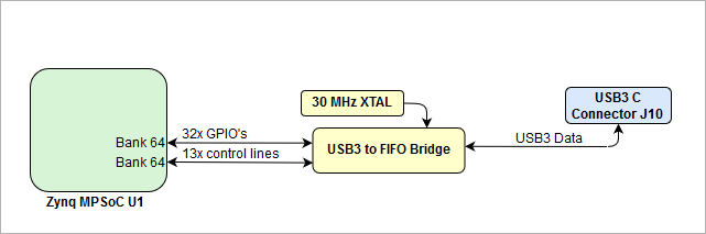 Image Added Image Added
|
|
The USB3 to FIFO bridge FTDI FT601Q U9 is connected to the Zynq MPSoC's PL bank 64 and is accessible through USB-C connector J10:
| Scroll Title |
|---|
| anchor | Table_x |
|---|
| title | Table x: FTDI SignalsUSB-C connector J10 |
|---|
|
| Scroll Table Layout |
|---|
| orientation | portrait |
|---|
| sortDirection | ASC |
|---|
| repeatTableHeaders | default |
|---|
| style | |
|---|
| widths | |
|---|
| sortByColumn | 1 |
|---|
| sortEnabled | false |
|---|
| cellHighlighting | true |
|---|
|
The USB3 to FIFO bridge U9 is connected to the Zynq MPSoC's PL bank 64 and is accessible through USB-C connector J10: | IC | Interface | Signal Schematic Names | Connected to | Notes | FT601Q U9
|---|
| USB3 data lane | - SSRX_P
- SSRX_N
- SSTXX_P
- SSTXX_N
| USB C Connector J10 | - | | USB2 data lane | | USB C Connector J10 | - | | Control Lines | - FTDI_RESET_N
- WAKEUP_N
- SIWU_N
- TXE_N
- RXF_N
- WR_N
- RD_N
- OE_N
- BE_0
- BE_1
- BE_2
- BE_3
- FIFO_CLK
| PL bank 64
| - | | Parallel GPIO's | | PL bank 64 | -32bit FIFO register |
|
See FT600Q-FT601Q IC Datasheet for interface details.
...
| Scroll Title |
|---|
| anchor | Figure_3 |
|---|
| title | Figure 3: JTAG/UART Interface |
|---|
|
| Scroll Ignore |
|---|
| draw.io Diagram |
|---|
| border | false |
|---|
| viewerToolbar | true |
|---|
| |
|---|
| fitWindow | false |
|---|
| diagramDisplayName | |
|---|
| lbox | true |
|---|
| revision | 8 |
|---|
| diagramName | uart_jtag |
|---|
| simpleViewer | truefalse |
|---|
| width | |
|---|
| links | auto |
|---|
| tbstyle | tophidden |
|---|
| diagramWidth | 642 |
|---|
|
|
| Scroll Only |
|---|
|
|
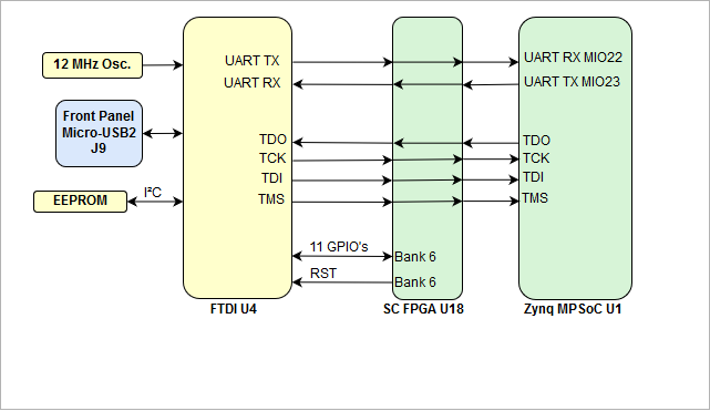
The USB2 to FIFO bridge FTDI FT2232H U4 is connected to the SC FPGA U18 and is accessible through Micro-USB2 connector J9:
| Scroll Title |
|---|
| anchor | Table_x |
|---|
| title | Table x: FTDI SignalsMicro-USB2 connector J9 |
|---|
|
| Scroll Table Layout |
|---|
| orientation | portrait |
|---|
| sortDirection | ASC |
|---|
| repeatTableHeaders | default |
|---|
| style | |
|---|
| widths | |
|---|
| sortByColumn | 1 |
|---|
| sortEnabled | false |
|---|
| cellHighlighting | true |
|---|
|
The USB2 to FIFO bridge U4 is connected to the SC FPGA U18 and is accessible through Micro-USB2 connector J9: | IC | Interface | Signal Schematic Names | Connected to | Notes | FT2232H U4 |
|---|
| USB2 data lane | | Micro-USB2 connector J9 | - | | Control Lines | | SC FPGA U18, bank 6
| - | | Parallel GPIO's | - ADBUS0
- ADBUS1
- ADBUS2
- ADBUS3
- BDBUS0
- BDBUS1
- BDBUS2
- BDBUS3
- BDBUS4
- BDBUS5
- BDBUS6
- BDBUS7
- BCBUS0
- BCBUS1
- BCBUS2
- BCBUS3
- BCBUS4
| SC FPGA U18, bank 6 | - |
|
...
| Scroll Title |
|---|
| anchor | Figure_3 |
|---|
| title | Figure 3: JTAG/UART Interface |
|---|
|
| Scroll Ignore |
|---|
| draw.io Diagram |
|---|
| border | truefalse |
|---|
| viewerToolbar | true |
|---|
| |
|---|
| fitWindow | false |
|---|
| diagramDisplayName | |
|---|
| lbox | true |
|---|
| revision | 2 |
|---|
| diagramName | TEC0850 SD IO |
|---|
| simpleViewer | false |
|---|
| width | |
|---|
| links | auto |
|---|
| tbstyle | hidden |
|---|
| diagramWidth | 641 | revision | 2 |
|---|
|
|
| Scroll Only |
|---|
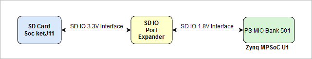 Image Added Image Added
|
|
There are some limitations to use SD card Interface in Linux.
...
| Scroll Title |
|---|
| anchor | Figure_3 |
|---|
| title | Figure 3: JTAG/UART Interface |
|---|
|
| Scroll Ignore |
|---|
| draw.io Diagram |
|---|
| border | truefalse |
|---|
| viewerToolbar | true |
|---|
| |
|---|
| fitWindow | false |
|---|
| diagramDisplayName | |
|---|
| lbox | true |
|---|
| revision | 2 |
|---|
| diagramName | TEC0850 GbE |
|---|
| simpleViewer | false |
|---|
| width | |
|---|
| diagramWidthlinks | 641auto |
|---|
| tbstyle | hidden |
|---|
| diagramWidth | 641 | revision | 1 |
|---|
|
|
| Scroll Only |
|---|
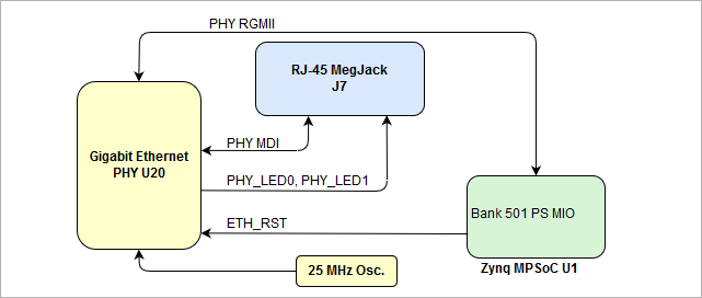 Image Added Image Added
|
|
DDR4 SODIMM Socket
On the TEC0850 board there is a DDR4 memory interface U3 with a 64-bit databus width available for SO-DIMM modules connected to the Zynq UltraScale+ DDRC hard memory controller.
| Scroll Title |
|---|
| anchor | Figure_3 |
|---|
| title | Figure 3: JTAG/UART Interface |
|---|
|
| Scroll Ignore |
|---|
| draw.io Diagram |
|---|
| border | truefalse |
|---|
| viewerToolbar | true |
|---|
| |
|---|
| fitWindow | false |
|---|
| diagramDisplayName | |
|---|
| lbox | true |
|---|
| revision | 1 |
|---|
| diagramName | TEC0850 DDR4 interface |
|---|
| simpleViewer | false |
|---|
| width | |
|---|
| links | auto |
|---|
| tbstyle | hidden |
|---|
| diagramWidth | 641 | revision
|---|
|
|
| Scroll Only |
|---|
1 | scroll-only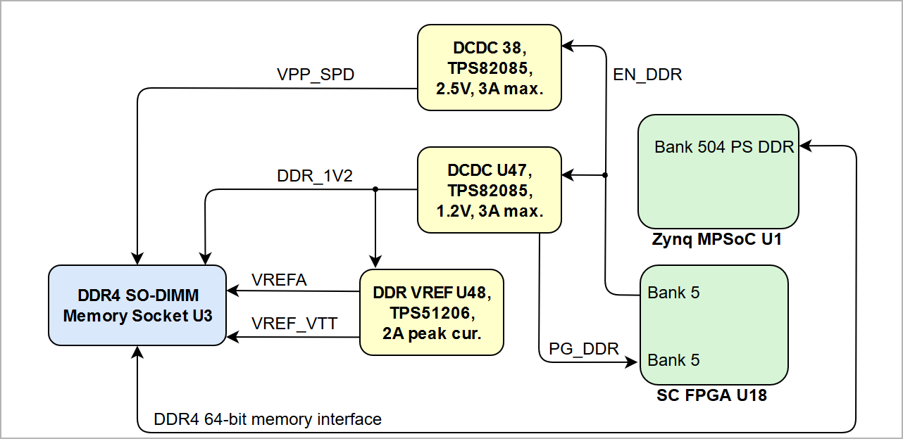 Image Added Image Added
|
|
Following table gives an overview about the memory interface I/O signals of the DDR4 SDRAM SO-DIMM Socket U3:
| Scroll Title |
|---|
| anchor | Table_x |
|---|
| title | Table x: FTDI SignalsDDR4 SDRAM SO-DIMM Socket U3 |
|---|
|
| Scroll Table Layout |
|---|
| orientation | portrait |
|---|
| sortDirection | ASC |
|---|
| repeatTableHeaders | default |
|---|
| style | |
|---|
| widths | |
|---|
| sortByColumn | 1 |
|---|
| sortEnabled | false |
|---|
| cellHighlighting | true |
|---|
|
Following table gives an overview about the I/O signals of the memory interface:
| Connector | DDR4 SDRAM I/O Signal | Signal Schematic Name | Connected to | Notes | DDR4 SO-DIMM Socket U3 |
|---|
| Address inputs | | PS DDR Bank 504 | - | Bank address inputs
| | - | | Bank group inputs | | - | | Differential clocks | - DDR4-CLK0_P
- DDR4-CLK0_N
- DDR4-CLK1_P
- DDR4-CLK1_N
| 2 x DDR4 clock | | Data input/output | | - | | Check bit input/output | | - | | Data strobe (differential) | - DDR4-DQS0_P
- DDR4-DQS0_N
- ...
- DDR4-DQS8_P
- DDR4-DQS8_N
| - | | Data mask and data bus inversion | | - | | Serial address inputs | | address range configuration on I²C bus | | Control Signals | | chip selest signal | | On-die termination enable | | nRESET | | Command and address parity input | | Clock enable | | CRC error flag | | Activation command input | | Temperature event | | I²C | | not connected | - |
|
Circular Push Pull Connector
The TEC0850 board provides 4x DAC analog voltage output on the 5-pin circular push/pull connector J15. Each of the DAC units consists of one Texas Instruments THS5641AIPW digital stable current source, TI THS4631D operational amplifier and LDOs, by which each of the DAC units can be switched on and off.
The TI THS4631D digital stable current source wired to the operational amplifier circuitry creating the DAC unit with a voltage output range from -0.5V ... 0.5V. See TI THS5641 datasheet and schematic how to control the DAC unit and to configure the analog output voltages on connector J15.
| Scroll Title |
|---|
| Scroll Title |
|---|
| anchor | Figure_11 |
|---|
| title | Figure 11: CAN interface |
|---|
|
| Scroll Ignore |
|---|
| draw.io Diagram |
|---|
| border | truefalse |
|---|
| viewerToolbar | true |
|---|
| |
|---|
| fitWindow | false |
|---|
| diagramDisplayName | |
|---|
| lbox | true |
|---|
| revision | 3 |
|---|
| diagramName | diagramName | TEC0850 DACs |
|---|
| simpleViewer | false |
|---|
| width | |
|---|
| links | auto |
|---|
| diagramWidthtbstyle | 595hidden |
|---|
| revisiondiagramWidth | 1641 |
|---|
|
|
|
There is a 26-pin
...
IDC header (2x13
...
3-Pin PicoBlade Connector
Battery holder
...
, 1.27mm grid size) J16 available on the TEC0850 board which exposes the 20 FPGA HD I/O's of PL bank 47 to the user. The PL bank 47 has 3.3V VCCO bank voltage, on the header J16 there also the voltage levels 3.3V and 5V available. The I/O's can be accessed with a corresponding IDC connector.
| Scroll Title |
|---|
| anchor | Figure_1311 |
|---|
| title | Figure 13: 4-wire PWM FAN connectors11: CAN interface |
|---|
|
| Scroll Ignore |
|---|
| draw.io Diagram |
|---|
| border | truefalse |
|---|
| viewerToolbar | true |
|---|
| |
|---|
| fitWindow | false |
|---|
| diagramDisplayName | |
|---|
| lbox | true |
|---|
| revision | 2 |
|---|
| diagramName | TEC0850 4-Wire PWM Connectorheader J16 |
|---|
| simpleViewer | false |
|---|
| width |
|---|
| diagramWidth | 641 |
|---|
| | links | auto |
|---|
| tbstyle | hidden |
|---|
| diagramWidth | 346 | revision | 2 |
|---|
|
|
|
...
...
On the TEC0850 there is a 10-pin SMT header (2x5, 2.54mm grid size) J13 present which provides access to the JTAG and UART interface of Altera MAX10 System Controller FPGA. The header J13 has a compatible pin assignment to the TEI0004 JTAG programmer for Altera FPGAs, the voltage levels 3.3V is on the header available as reference I/O-voltage for JTAG and UART.
The 4 JTAG pins of the header J13 are also connected to the cPCI connector J1 and can be used es user GPIO's of the SC FPGA U18 with othr functionalities then JTAG.
On the header J13 there is also a reference clock signal from PLL clcok U14 available, which can be also used for the SC FPGA U18 and on the cPCI connector J1.
| Scroll Title |
|---|
| anchor | Figure_11 |
|---|
| title | Figure 11: CAN interface |
|---|
|
| Scroll Ignore |
|---|
| draw.io Diagram |
|---|
| border | false |
|---|
| viewerToolbar | true |
|---|
| |
|---|
| fitWindow | false |
|---|
| diagramDisplayName | |
|---|
| lbox | true |
|---|
| revision | 3 |
|---|
| diagramName | TEC0850 header 13 |
|---|
| simpleViewer | false |
|---|
| width | |
|---|
| links | auto |
|---|
| tbstyle | hidden |
|---|
| diagramWidth | 641 |
|---|
|
|
|
3-Pin PicoBlade Connector
2 I/O's of the SC FPGA U18 are exposed to the on-board 3-Pin PicoBlade header J8 available to the user or for future use of upcoming versions of SC FPGA firmware.
| Scroll Title |
|---|
| anchor | Figure_11 |
|---|
| title | Figure 11: CAN interface |
|---|
|
| Scroll Ignore |
|---|
| draw.io Diagram |
|---|
| border | false |
|---|
| viewerToolbar | true |
|---|
| |
|---|
| fitWindow | false |
|---|
| diagramDisplayName | |
|---|
| lbox | true |
|---|
| revision | 3 |
|---|
| diagramName | TEC0850 header J8 |
|---|
| simpleViewer | false |
|---|
| width | |
|---|
| links | auto |
|---|
| tbstyle | hidden |
|---|
| diagramWidth | 641 |
|---|
|
|
|
Battery Holder
There is a CR1220 battery holder available to the supply the voltage for the for for the Zynq MPSoC's Battery Power Domain (BBRAM and RTC). The battery voltage VBATT should be in the range of 2.2V to 5.5V, use 3.0V CR1220 battery.
| Scroll Title |
|---|
| anchor | Figure_11 |
|---|
| title | Figure 11: CAN interface |
|---|
|
| Scroll Ignore |
|---|
| draw.io Diagram |
|---|
| border | false |
|---|
| viewerToolbar | true |
|---|
| |
|---|
| fitWindow | false |
|---|
| diagramDisplayName | |
|---|
| lbox | true |
|---|
| revision | 4 |
|---|
| diagramName | TEC0850 battery holder |
|---|
| simpleViewer | false |
|---|
| width | |
|---|
| links | auto |
|---|
| tbstyle | hidden |
|---|
| diagramWidth | 641 |
|---|
|
|
|
4-Wire PWM FAN Connectors
The TEC0850 offers one 4-wire PWM FAN connector FPGA cooling fan controlled by SC FPGA U18:
| Scroll Title |
|---|
| anchor | Figure_13 |
|---|
| title | Figure 13: 4-wire PWM FAN connectors |
|---|
|
| Scroll Ignore |
|---|
| draw.io Diagram |
|---|
| border | false |
|---|
| viewerToolbar | true |
|---|
| |
|---|
| fitWindow | false |
|---|
| diagramDisplayName | |
|---|
| lbox | true |
|---|
| revision | 2 |
|---|
| diagramName | TEC0850 4-Wire PWM Connector |
|---|
| simpleViewer | false |
|---|
| width | |
|---|
| links | auto |
|---|
| tbstyle | hidden |
|---|
| diagramWidth | 641 |
|---|
|
|
| Scroll Only |
|---|
 Image Added Image Added
|
|
On-board Peripherals
| Page properties |
|---|
|
Notes : - add subsection for every component which is important for design, for example:
- Ethernet PHY
- USB PHY
- Programmable Clock Generator
- Oscillators
- eMMCs
- RTC
- FTDI
- ...
- DIP-Switches
- Buttons
- LEDs
|
Zynq UltraScale XCZU15EG MPSoC
The TEC0850 board is populated with the Zynq UltraScale+ XCZU15EG-1FFVB1156E MPSoC.
The PS MIO pins are routed to the on-board peripherals as follows:
| Scroll Title |
|---|
| anchor | Table_x |
|---|
| title | Table x: Default MIO Configuration |
|---|
|
| Scroll Table Layout |
|---|
| orientation | portrait |
|---|
| sortDirection | ASC |
|---|
| repeatTableHeaders | default |
|---|
| style | |
|---|
| widths | |
|---|
| sortByColumn | 1 |
|---|
| sortEnabled | false |
|---|
| cellHighlighting | true |
|---|
|
| PS MIO | Function | Connected to |
|---|
| 0 | SPI0 | U24-B2, CLK |
|---|
| 1 | SPI0 | U24-D2, DO/IO1
|
|---|
| 2 | SPI0 | U24-C4, WP/IO2
|
|---|
| 3 | SPI0 | U24-D4, HOLD/IO3 |
|---|
| 4 | SPI0 | U24-D3, DI/IO0 |
|---|
| 5 | SPI0 | U24-C2, CS |
|---|
| 6 | - | Not connected |
|---|
| 7 | SPI1 | U25-C2, CS |
|---|
| 8 | SPI1 | U25-D3, DI/IO0 |
|---|
| 9 | SPI1 | U25-D2, DO/IO1 |
|---|
| 10 | SPI1 | U17-C4, WP/IO2 |
|---|
| 11 | SPI1 | U25-D4, HOLD/IO3 |
|---|
| 12 | SPI1 | U25-B2, CLK |
|---|
| 13 ... 15 | - | not connected |
|---|
| 16 | USB2 PHY Reset | USB2 PHY U11 |
|---|
| 17 | - | not used |
|---|
| 18 ... 19 | - | not connected |
|---|
| 20 ...21 | PS MIO I²C | I²C peripherals |
|---|
| 22 ... 25 | user MIO | SC FPGA U18, bank 2 |
|---|
| 26 ... 38 | RGMII | GbE PHY U20 |
|---|
| 39 ... 44 | - | not connected |
|---|
| 45 ... 51 | SD IO | MicroSD Card socket J11 |
|---|
| 52 ... 63 | USB2 ULPI | USB2 PHY U11 |
|---|
| 64 ... 75 | - | not used |
|---|
| 76 ... 77 | ETH MDC / MDIO | GbE PHY U20 |
|---|
|
MAX10 System Controller FPGA
The TEC0850 board is equipped with one System Controller FPGA (Intel MAX10 10M08SAU169C8G) with the schematic designators U18. The SC FPGA is the central system management unit where essential control signals are logically linked by the implemented logic in FPGA firmware, which generates output signals to control the system, the on-board peripherals and the interfaces. Interfaces like JTAG and UART between the FTDI FT2232H chip and to the Zynq MPSoC are by-passed, forwarded and controlled by the System Controller FPGA.
Other tasks of the System Controller FPGA are the monitoring of the power-on sequence and to display the programming state of the FPGA module. The functionalities and configuration of the pins depend on the SC FPGA's firmware. The documentation of the firmware of SC FPGA U18 contains detailed information on this matter.
The Sytem Controller FPGA is connected to the Zynq Ultrascale+ MPSoC through MIO and PL pins. The signals of these pins are forwarded by the SC FPGA to control some of the on board peripherals.
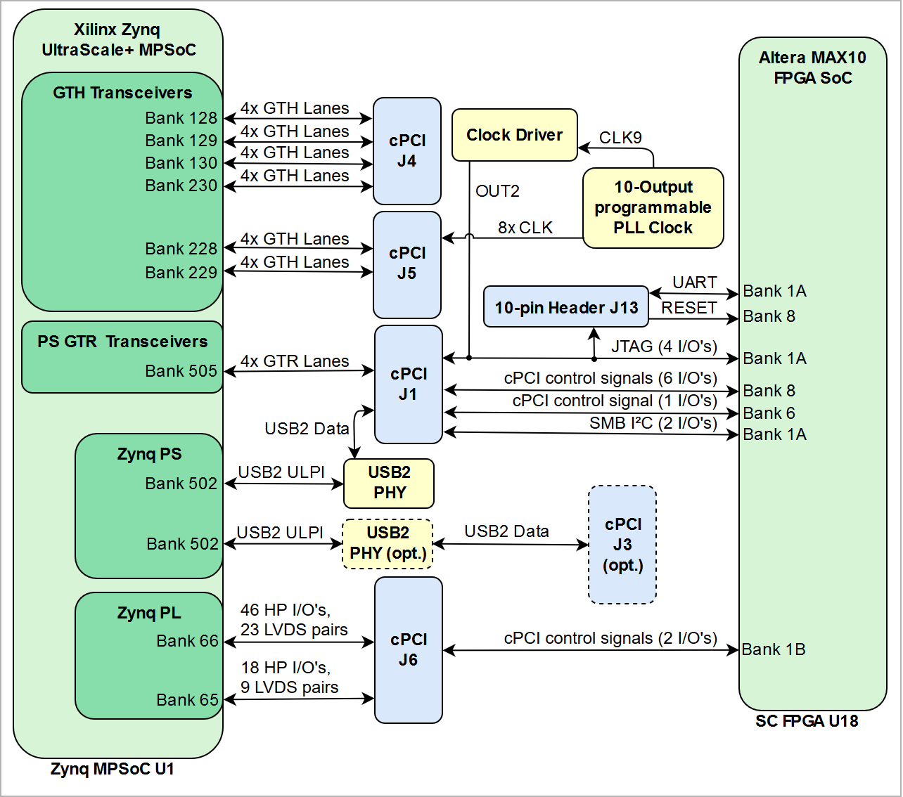
Following block diagram visualizes the connection of the SC FPGA with the Zynq Ultrascale+ MPSoC via PS MIO, PS Config and singled ended PL pins:
| Scroll Title |
|---|
| anchor | Figure_2 |
|---|
| title | Figure 2: TEF1001-02 main components |
|---|
|
| Scroll Ignore |
|---|
| draw.io Diagram |
|---|
| border | true |
|---|
| viewerToolbar | true |
|---|
| |
|---|
| fitWindow | false |
|---|
| diagramName | TEC0850 SC TO Zynq connections |
|---|
| simpleViewer | false |
|---|
| width | |
|---|
| diagramWidth | 641 |
|---|
| revision | 2 |
|---|
|
|
|
Programmable Clock Generator
There is a Si5345A U14, Silicon Labs I2C programmable 10-output PLL clock generator on-board to generate various reference clocks for the Zynq MPSoC MGT banks and on-board peripherals.
| Scroll Title |
|---|
| anchor | Figure_2 |
|---|
| title | Figure 2: TEF1001-02 main components |
|---|
|
| Scroll Ignore |
|---|
| draw.io Diagram |
|---|
| border | true |
|---|
| viewerToolbar | true |
|---|
| |
|---|
| fitWindow | false |
|---|
| diagramName | TEC0850 clock sourdes |
|---|
| simpleViewer | false |
|---|
| width | |
|---|
| diagramWidth | 641 |
|---|
| revision | 4 |
|---|
|
|
|
Following table shows on-board Silicon Labs I2C programmable Si5345A U17 10-output programmable PLL reference clock generator inputs and outputs:
| Scroll Title |
|---|
| anchor | Table_x |
|---|
| title | Table x: SI5345 I2C address |
|---|
|
| Scroll Table Layout |
|---|
| orientation | portrait |
|---|
| sortDirection | ASC |
|---|
| repeatTableHeaders | default |
|---|
| style | |
|---|
| widths | |
|---|
| sortByColumn | 1 |
|---|
| sortEnabled | false |
|---|
| cellHighlighting | true |
|---|
|
Si5345A U14 Pin
| Signal Schematic Name
| Connected to | Clock Direction | Note |
|---|
| IN0 | | 40.000 MHz Oscillator U75 | Input | external reference
clock input | | GND | | IN1 | - | not connected | Input | not used | | - | not connected | | IN2 | - | not connected | Input | not used | | - | not connected | | IN3 | - | not connected | Input | not used
| | - | not connected | | OUT0 | | Quad clock buffer
Si53340 U16 | Output | reference clock input to
Quad clock buffer | | | OUT1 | | cPCI J5, pin B5 | Output | reference clock output
to cPCI connector J5 | | cPCI J5, pin A5 | | OUT2 | | cPCI J5, pin C6 | Output | | cPCI J5, pin B6 | | OUT3 | | cPCI J5, pin E5 | Output | | cPCI J5, pin D5 | | OUT4 | | cPCI J5, pin H5 | Output | | cPCI J5, pin G5 | | OUT5 | | cPCI J5, pin K5 | Output | | cPCI J5, pin J5 | | OUT6 | | cPCI J5, pin F6 | Output | | cPCI J5, pin E6 | | OUT7 | | cPCI J5, pin L6 | Output | | cPCI J5, pin K6 | | OUT8 | | cPCI J5, pin I6 | Output | | cPCI J5, pin H6 | | OUT9 | | Clock Driver LTC6975 U73 | Output | reference clock input to
dual clock driver | | | XA/XB | | 54.000 MHz quartz
oscillator Y3 | Input | Differential quartz oscillator
clock input | |
|
The clock outputs OUT1 and OUT9 are distributed via clock buffer U16 and clock driver U14 to several PL and MGT banks:
| Scroll Title |
|---|
| anchor | Table_x |
|---|
| title | Table x: SI5345 I2C address |
|---|
|
| Scroll Table Layout |
|---|
| orientation | portrait |
|---|
| sortDirection | ASC |
|---|
| repeatTableHeaders | default |
|---|
| style | |
|---|
| widths | |
|---|
| sortByColumn | 1 |
|---|
| sortEnabled | false |
|---|
| cellHighlighting | true |
|---|
|
Si53340 U16 Pin
| Signal Schematic Name
| Connected to | Clock Direction | Note |
|---|
| Q0 | | | Output | GTH bank 229 reference clock input | | Q1 | | | Output | PL HP bank 66 reference clock input | | Q2 | | | Output | PS GTR Bank 505 reference clock input | | Q3 | | | Output | GTH bank 129 reference clock input | | LTC6957 U14 Pin |
|
|
|
|
|---|
| OUT1 | | | Output | PL HP bank 65 reference clock input | | OUT2 | | - Signal 'SATA_SL'
- Signal 'SATA_SCL'
| Output | reference clock input cPCI connector J1,
header J13 and SC FPGA U18 |
|
The clock generator U14 is programmable via the on-board I²C bus connected to MIO 20...21 pins. The I²C address is shown in the table below.
...
| Page properties |
|---|
|
Notes : - add subsection for every component which is important for design, for example:
- Ethernet PHY
- USB PHY
- Programmable Clock Generator
- Oscillators
- eMMCs
- RTC
- FTDI
- ...
- DIP-Switches
- Buttons
- LEDs
|
Subsections...
Zynq UltraScale XCZU15EG MPSoC
The TEC0850 board is populated with the Zynq UltraScale+ XCZU15EG-1FFVB1156E MPSoC.
Main IO interfaces are shown on the image below.
PS MIO Configuration
| Scroll Title |
|---|
| anchor | Table_x |
|---|
| title | Table x: Default MIO ConfigurationSI5345 I2C address |
|---|
|
| Scroll Table Layout |
|---|
| orientation | portrait |
|---|
| sortDirection | ASC |
|---|
| repeatTableHeaders | default |
|---|
| style | |
|---|
| widths | |
|---|
| sortByColumn | 1 |
|---|
| sortEnabled | false |
|---|
| cellHighlighting | true |
|---|
|
|
| MIO | Interface |
|---|
| MIO 0...12 | QSPI Flash Memory |
| MIO 20...21 | I2C 1 |
| MIO 22...23 | UART 0 |
| MIO 26...37 | GEM 0 |
| MIO 46...51 | SD 1 |
| MIO 52...63 | USB 0 |
| MIO 64...75 | USB 1 |
| MIO 76...77 | MDIO 0 |
MAX10 System Controller
System controller chip is Intel MAX10 10M08SAU169C8G Chip with board control firmware.
...
| I2C address | Chip | Description |
|---|
| 0x69 | U14 Si5345 | Clock generator and distributor |
|
Oscillators
The TEC0850 board is equipped several on-board oscillators to provide the Zynq Ultrascale+ MPSoC's PS and PL banks and the on-board peripherals with reference clock-signals:
| Scroll Title |
|---|
| anchor | FigureTable_2x |
|---|
| title | Figure 2: TEF1001-02 main componentsTable x: SI5345 I2C address |
|---|
|
ignore| draw.io Diagram |
|---|
|
| border | false |
|---|
| viewerToolbar | true |
|---|
| fitWindow | false |
|---|
diagramDisplayName | | lbox | true |
|---|
| revision | 3 |
|---|
| diagramName | Clocks Diagram |
|---|
| simpleViewer | true |
|---|
width | | links | auto |
|---|
| tbstyle | top |
|---|
| diagramWidth | 641 |
|---|
| Scroll Only |
|---|
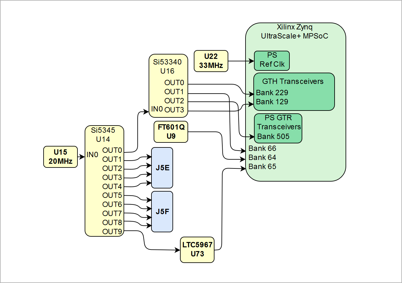 Image Removed Image Removed
|
I2C
The onboard I2C bus is connected to MIO 20...21 pins. Devices on the bus shown in the table below.
...
| anchor | Table_x |
|---|
| title | Table x: SI5345 I2C address |
|---|
...
| tablelayout |
|---|
| orientation | portrait |
|---|
| sortDirection | ASC |
|---|
| repeatTableHeaders | default |
|---|
| style | |
|---|
| widths | |
|---|
| sortByColumn | 1 |
|---|
| sortEnabled | false |
|---|
| cellHighlighting | true |
|---|
|
| Clock Source | Signal Schematic Name | Frequency | Clock Input Destination |
|---|
| SiTime SiT8008BI oscillator, U22 | | 33.333333 MHz | Zynq MPSoC U1 PS Config Bank 503, pin U24 | | SiTime SiT8008AI oscillator, U12 | | 52.000000 MHz | USB2 transceiver PHY U11, pin 26 | | SiTime SiT8008AI oscillator, U16 | | 12.000000 MHz | FTDI FT2232H U4, pin 3 | | Kyocera CX3225SB30000, Y1 | - | 30.000 MHz | FTDI FT601Q U9, pin 21/22 | | CM-2012-2pad, Y2 | - | 32.768000 kHz | Zynq MPSoC U1 PS Config Bank 503, pin V21/V22 | | Kyocera CX3225SB26000, Y3 | | 54.000 MHz | 10-output PLL clock generator U14, pin 8/9 | | SiTime SiT8008BI oscillator, U21 | | 25.000000 MHz | Gigabit Ethernet PHY U20, pin 34 | | ASVTX-12-A oscillator, U75 | | 40.000 MHz | 10-output PLL clock generator U14, pin 63 |
|
FTDIs
FT2232H
FT601Q
Oscillators
FTDIs
FT2232H
FT601Q-B-T
Quad-SPI Flash Memory
Board has two N25Q512A11G1240E connected in a dual parallel mode.
EEPROMs
...
The onboard I2C bus is clock generator U14 is programmable via the on-board I²C bus connected to MIO 20...21 pins. Devices on the bus The I²C address is shown in the table below.
...
| Scroll Title |
|---|
| anchor | Figure_3 |
|---|
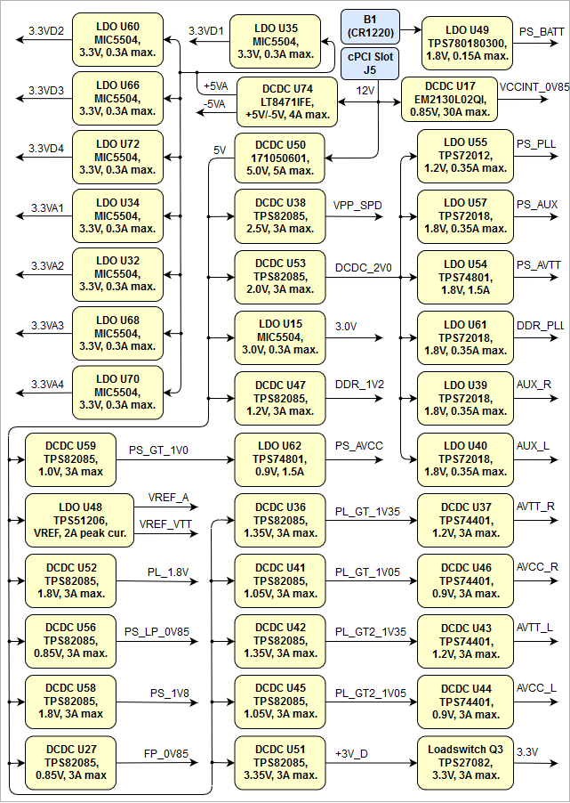
| title | Figure 3: Power Distribution |
|---|
|
| Scroll Ignore |
|---|
| draw.io Diagram |
|---|
| border | false |
|---|
| viewerToolbar | true |
|---|
| |
|---|
| fitWindow | false |
|---|
| diagramDisplayName | |
|---|
| lbox | true |
|---|
| revision | 16 |
|---|
| diagramName | Power supply |
|---|
| simpleViewer | truefalse |
|---|
| width | |
|---|
| links | auto |
|---|
| tbstyle | hidden |
|---|
| diagramWidth | 641 |
|---|
|
|
| Scroll Only |
|---|
|
|
...
On the TEB0911 UltraRack board following Power Domains will be powered up in a certain sequence with by enable and power-good signals of the DC-DC converters, which are controlled by the System Controller FPGA U18:
- Main Power and Programmable Logic (PL)
- Low-Power Domain (LPD)
- Programmable Logic (PL) and Full-Power Domain (FPD)
- GTH, PS GTR transceiver and DDR memory
- Optional DAC voltages
Hence, those three power instances will be powered up consecutively when the Power-Good signals of the previous instance is asserted.
...
| Scroll Title |
|---|
| anchor | Figure_x |
|---|
| title | Figure x: Physical dimensions drawing |
|---|
|
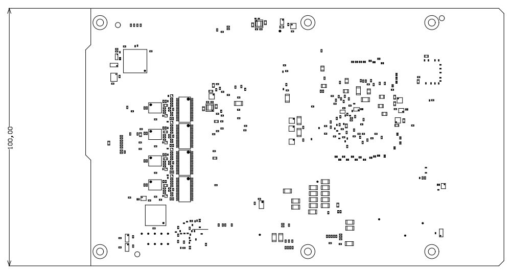 Image Added Image Added
|
Variants Currently In Production
...