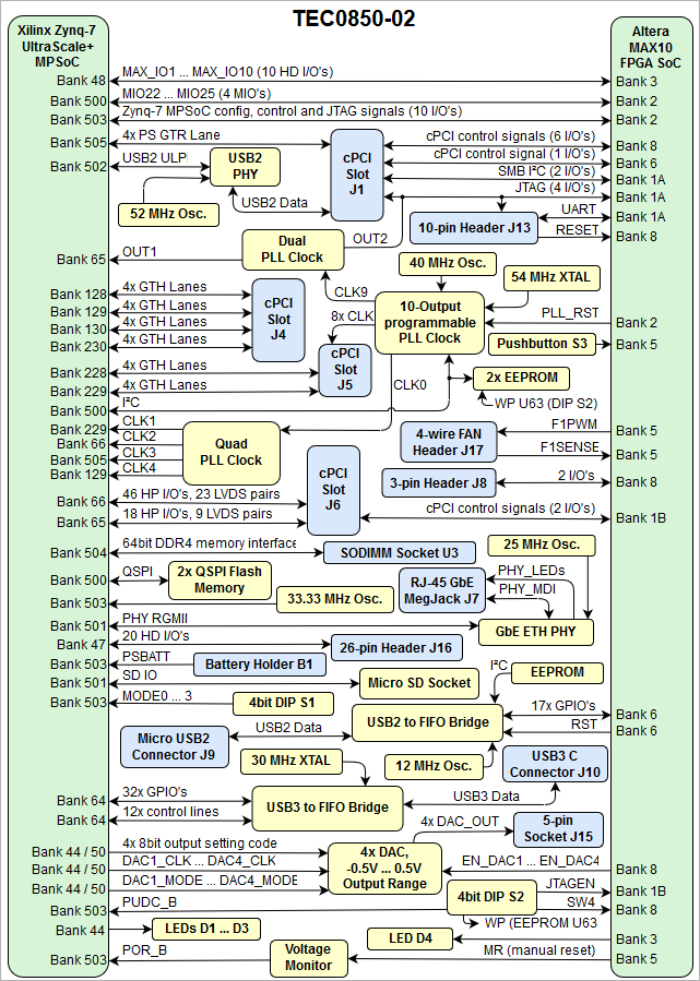
...
| Scroll Title |
|---|
| anchor | Figure_1 |
|---|
| title | Figure 1: TEC0850-02 block diagram |
|---|
|
| Scroll Ignore |
|---|
| draw.io Diagram |
|---|
| border | false |
|---|
| viewerToolbar | true |
|---|
| |
|---|
| fitWindow | false |
|---|
| diagramDisplayName | |
|---|
| lbox | true |
|---|
| revision | 23 |
|---|
| diagramName | TEC0850 overview |
|---|
| simpleViewer | false |
|---|
| width | |
|---|
| links | auto |
|---|
| tbstyle | hidden |
|---|
| diagramWidth | 641 |
|---|
|
|
| Scroll Only |
|---|
|
|
...
The TEC0850 board provides 4x DAC analog voltage output on the 5-pin circular push/pull connector J15. Each of the DAC units consists of one Texas Instruments THS5641AIPW digital stable current sourceto analog converter, TI THS4631D operational amplifier and two LDOs, by which each of the DAC units unit can be switched on and off.
The TI THS4631D digital stable current source to analog converter wired to the operational amplifier circuitry creating the DAC unit with a voltage output range from -0.5V ... 0.5V. See TI THS5641 datasheet and schematic how to control the DAC unit and to configure set the analog output voltages on connector J15.
...
| Scroll Title |
|---|
| anchor | Figure_11 |
|---|
| title | Figure 11: CAN interface |
|---|
|
| Scroll Ignore |
|---|
| draw.io Diagram |
|---|
| border | false |
|---|
| viewerToolbar | true |
|---|
| |
|---|
| fitWindow | false |
|---|
| diagramDisplayName | |
|---|
| lbox | true |
|---|
| revision | 34 |
|---|
| diagramName | TEC0850 FT2232H |
|---|
| simpleViewer | false |
|---|
| width | |
|---|
| links | auto |
|---|
| tbstyle | hidden |
|---|
| diagramWidth | 641 |
|---|
|
|
|
...
The TEC0850 board is equipped with the FTDI FT601Q USB3 to 32bit-FIFO adapter controller connected to USB-C connector J10 to provide access to the Zynq MPSoC PL HP I/O's of bank 64. Also 12 13 control signals of the FTDI FT601Q are connected to the HP bank 64.
| Scroll Title |
|---|
| anchor | Table_x |
|---|
| title | Table x: SI5345 I2C address |
|---|
|
| Scroll Table Layout |
|---|
| orientation | portrait |
|---|
| sortDirection | ASC |
|---|
| repeatTableHeaders | default |
|---|
| style | |
|---|
| widths | |
|---|
| sortByColumn | 1 |
|---|
| sortEnabled | false |
|---|
| cellHighlighting | true |
|---|
|
| FT601Q U9 Pin | Signal Schematic Name | Connected to | Notes |
|---|
| Pin 1240, ADBUS0 DATA0 | DATA | SC FPGA U18 bank 6DATA0 | PL HP bank 64, pin | G9AK1 | user | configurableGPIO's | | Pin 1341, ADBUS1 DATA1 | DATA | SC FPGA U18 bank 6DATA1 | PL HP bank 64, pin | F10AJ10 | | Pin 1442, ADBUS2 DATA2 | DATA | SC FPGA U18 bank 6DATA2 | PL HP bank 64, pin | E10AJ9
| | Pin 1543, ADBUS3 DATA3 | DATA | SC FPGA U18 bank 6DATA3 | PL HP bank 64, pin | D9AK7 | | Pin 3244, BDBUS0 DATA4 | DATA | SC FPGA U18 bank 6DATA4 | PL HP bank 64, pin | B11AK5
| | Pin 3345, BDBUS1 DATA5 | DATA | SC FPGA U18 bank 6DATA5 | PL HP bank 64, pin | A12AM1
| | Pin 3446, BDBUS2 DATA6 | DATA | SC FPGA U18 bank 6DATA6 | PL HP bank 64, pin | B12AL2
| | Pin 3547, BDBUS3 DATA7 | DATA | SC FPGA U18 bank 6DATA7 | PL HP bank 64, pin | C11AK4 | | Pin 3750, BDBUS4 DATA8 | DATA | SC FPGA U18 bank 6DATA8 | PL HP bank 64, pin | B13AN1 | | Pin 3851, BDBUS5 DATA9 | DATADATA | SC FPGA U18 bank 6DATA9 | PL HP bank 64, pin | C12AL3
| | Pin 3952, BDBUS6 DATA10 | BDBUS6 | SC FPGA U18 bank 6DATA10 | PL HP bank 64, pin | C13AK8 | | Pin 4053, BDBUS7 DATA11 | BDBDATAUS7 | SC FPGA U18 bank 6DATA11 | PL HP bank 64, pin | D11AN2 | | Pin 4254, BCBUS0 DATA12 | BCBUS0 | SC FPGA U18 bank 6DATA12 | PL HP bank 64, pin | D12AP2 | | Pin 4655, BCBUS1 DATA13 | BCBUS1 | SC FPGA U18 bank 6DATA13 | PL HP bank 64, pin | E13AL7 | | Pin 4756, BCBUS2 DATA14 | BCBUS2 | SC FPGA U18 bank 6DATA14 | PL HP bank 64, pin | E12AL5 | | Pin 4857, BCBUS3 DATA15 | BCBUS3 | SC FPGA U18 bank 6DATA15 | PL HP bank 64, pin | F13AM4 | | Pin 4960, BCBUS4 DATA16 | BCBUS4 | SC FPGA U18 bank 6, pin F12 |
|
Quad-SPI Flash Memory
On-board QSPI flash memory U24 and U25 on the TEC0850 board is provided by Micron Serial NOR Flash Memory N25Q256A with 256 Mbit (32 MByte) storage capacity each, 64 MByte total QSPI Flash memory. The QSPI Flash memory ICs are connected to the PS MIO bank (Dual QSPI MIO0 ... MIO12) of the Zynq Ultrascale+ MPSoC, enabling dual parallel booting from QSPI Flash memory. This non volatile memory is used to store initial FPGA configuration. Besides FPGA configuration, remaining free flash memory can be used for user application and data storage. All four SPI data lines are connected to the Zynq MPSoC allowing x1, x2 or x4 data bus widths. Maximum data rate depends on the selected bus width and clock frequency used.
...
| anchor | Figure_11 |
|---|
| title | Figure 11: CAN interface |
|---|
...
| anchor | Table_x |
|---|
| title | Table x: SI5345 I2C address |
|---|
...
QSPI Flash U24,
N25Q256A11E1240E
...
MIO0
...
MIO1
...
MIO2
...
MIO3
...
MIO4
...
MIO5
...
QSPI Flash U25,
N25Q256A11E1240
...
MIO7
...
| DATA16 | PL HP bank 64, pin AN4 | | Pin 61, DATA17 | DATA17 | PL HP bank 64, pin AM5
| | Pin 62, DATA18 | DATA18 | PL HP bank 64, pin AM6 | | Pin 63, DATA19 | DATA19 | PL HP bank 64, pin AN3 | | Pin 64, DATA20 | DATA20 | PL HP bank 64, pin AP3
| | Pin 65, DATA21 | DATA21 | PL HP bank 64, pin AP4 | | Pin 66, DATA22 | DATA22 | PL HP bank 64, pin AP5
| | Pin 67, DATA23 | DATA23 | PL HP bank 64, pin AN6
| | Pin 69, DATA24 | DATA24 | PL HP bank 64, pin AN7
| | Pin 70, DATA25 | DATA25 | PL HP bank 64, pin AP6 | | Pin 71, DATA26 | DATA26 | PL HP bank 64, pin AP7
| | Pin 72, DATA27 | DATA27 | PL HP bank 64, pin AP11 | | Pin 73, DATA28 | DATA28 | PL HP bank 64, pin AP10 | | Pin 74, DATA29 | DATA29 | PL HP bank 64, pin AP9
| | Pin 75, DATA30 | DATA30 | PL HP bank 64, pin AN9
| | Pin 76, DATA31 | DATA31 | PL HP bank 64, pin AP8 | | Pin 58, CLK | FIFO_CLK | PL HP bank 64, pin AL6 | control signals | | Pin 4, BE0 | BE_0 | PL HP bank 64, pin AM10
| | Pin 5, BE1 | BE_1 | PL HP bank 64, pin AK10 | | Pin 6, BE2 | BE_2 | PL HP bank 64, pin AM11
| | Pin 7, BE3 | BE_3 | PL HP bank 64, pin AL11
| | Pin 13, nOE | OE_N | PL HP bank 64, pin AL8
| | Pin 12, nRD | RD_N | PL HP bank 64, pin AK9
| | Pin 11, nWR | WR_N | PL HP bank 64, pin AM9
| | Pin 8, nTXE | TXE_N | PL HP bank 64, pin AK12 | | Pin 9, nRXN | RXF_N | PL HP bank 64, pin AJ12
| | Pin 10, nSIWU | SIWU_N | PL HP bank 64, pin AL10 | | Pin 15, nRESET | FTDI_RESET_N | PL HP bank 64, pin AM8
| | Pin 16, nWAKEUP | WAKEUP_N | PL HP bank 64, pin AN8
|
|
Quad-SPI Flash Memory
On-board QSPI flash memory U24 and U25 on the TEC0850 board is provided by Micron Serial NOR Flash Memory N25Q256A with 256 Mbit (32 MByte) storage capacity each, 64 MByte total QSPI Flash memory. The QSPI Flash memory ICs are connected to the PS MIO bank (Dual QSPI MIO0 ... MIO12) of the Zynq Ultrascale+ MPSoC, enabling dual parallel booting from QSPI Flash memory. This non volatile memory is used to store initial FPGA configuration. Besides FPGA configuration, remaining free flash memory can be used for user application and data storage. All four SPI data lines are connected to the Zynq MPSoC allowing x1, x2 or x4 data bus widths. Maximum data rate depends on the selected bus width and clock frequency used.
EEPROMs
The TEC0850 board contains several EEPROMs for configuration and general user purposes. The EEPROMs are provided by Microchip, the I²C interfaces is connected to Zynq MPSoC bank 502 MIO 20...21 pins:
| Scroll Title |
|---|
| anchor | Figure_11 |
|---|
| title | Figure 11: CAN interface |
|---|
|
| Scroll Ignore |
|---|
| draw.io Diagram |
|---|
| border | true |
|---|
| viewerToolbar | true |
|---|
| |
|---|
| fitWindow | false |
|---|
| diagramName | TEC0850 USB3 to FIFOQSPI Flash |
|---|
| simpleViewer | false |
|---|
| width | |
|---|
| diagramWidth | 641 |
|---|
| revision | 21 |
|---|
|
|
|
...
| Scroll Title |
|---|
| anchor | Table_x |
|---|
| title | Table x: EEPROMs SI5345 I2C Addressesaddress |
|---|
|
| Scroll Table Layout |
|---|
| orientation | portrait |
|---|
| sortDirection | ASC |
|---|
| repeatTableHeaders | default |
|---|
| style | |
|---|
| widths | |
|---|
| sortByColumn | 1 |
|---|
| sortEnabled | false |
|---|
| cellHighlighting | true |
|---|
|
|
| I2C address | Chip | Description |
|---|
| 0x50 | U63 24AA128T-I/ST | 128K Serial EEPROM |
| 0x53 | U64 24AA025E48T-I/OT | 2K Serial EEPROM with EUI-48™ or EUI-64™ Node Identity |
USB PHY
USB2 PHY U15 is provided by USB3320 from Microchip. The ULPI interface is connected to the Zynq Ultrascale+ PS USB0. I/O voltage is fixed at 1.8V and PHY reference clock input is supplied from the on-board 52.000000 MHz oscillator U12.
...
| anchor | Figure_11 |
|---|
| title | Figure 11: CAN interface |
|---|
...
| anchor | Table_x |
|---|
| title | Table x: EEPROMs I2C Addresses |
|---|
...
Zynq MPSoC MIO16, pin AM16
...
| IC | Memory Density | MIO | Signal Schematic Name | Flash Memory Pin |
|---|
QSPI Flash U24, N25Q256A11E1240E | 256 Mbit (32 MByte) | 0 | MIO0 | B2 | | 1 | MIO1 | D2 | | 2 | MIO2 | C4 | | 3 | MIO3 | D4 | | 4 | MIO4 | D3 | | 5 | MIO5 | C2 | QSPI Flash U25, N25Q256A11E1240 | 256 Mbit (32 MByte) | 7 | MIO7 | C2 | | 8 | MIO8 | D3 | | 9 | MIO9 | D2 | | 10 | MIO10 | C4 | | 11 | MIO11 | D4 | | 12 | MIO12 | B2 |
|
EEPROMs
The TEC0850 board contains several EEPROMs for configuration and general user purposes. The EEPROMs are provided by Microchip, the I²C interfaces is connected to Zynq MPSoC bank 502 MIO 20...21 pins:
| Scroll Title |
|---|
| anchor | Figure_11 |
|---|
| title | Figure 11: CAN interface |
|---|
|
| Scroll Ignore |
|---|
| draw.io Diagram |
|---|
| border | true |
|---|
| viewerToolbar | true |
|---|
| |
|---|
| fitWindow | false |
|---|
| diagramName | TEC0850 USB3 to FIFO |
|---|
| simpleViewer | false |
|---|
| width | |
|---|
| diagramWidth | 641 |
|---|
| revision | 2 |
|---|
|
|
|
The EEPROMs U63 and U64 are programmable via the on-board I²C bus connected to MIO 20...21 pins. The I²C address is shown in the table below.
| Scroll Title |
|---|
| anchor | Table_x |
|---|
| title | Table x: EEPROMs I2C Addresses |
|---|
|
| Scroll Table Layout |
|---|
| orientation | portrait |
|---|
| sortDirection | ASC |
|---|
| repeatTableHeaders | default |
|---|
| style | |
|---|
| widths | |
|---|
| sortByColumn | 1 |
|---|
| sortEnabled | false |
|---|
| cellHighlighting | true |
|---|
|
| I2C address | Chip | Description |
|---|
| 0x50 | U63 24AA128T-I/ST | 128K Serial EEPROM | | 0x53 | U64 24AA025E48T-I/OT | 2K Serial EEPROM with EUI-48™ or EUI-64™ Node Identity |
|
USB2 PHY
USB2 PHY U15 is provided by USB3320 from Microchip. The ULPI interface is connected to the Zynq Ultrascale+ PS USB0. I/O voltage is fixed at 1.8V and PHY reference clock input is supplied from the on-board 52.000000 MHz oscillator U12.
| Scroll Title |
|---|
| anchor | Figure_11 |
|---|
| title | Figure 11: CAN interface |
|---|
|
| Scroll Ignore |
|---|
| draw.io Diagram |
|---|
| border | true |
|---|
| viewerToolbar | true |
|---|
| |
|---|
| fitWindow | false |
|---|
| diagramName | TEC0850 USB2 PHY |
|---|
| simpleViewer | false |
|---|
| width | |
|---|
| diagramWidth | 641 |
|---|
| revision | 1 |
|---|
|
|
|
| Scroll Title |
|---|
| anchor | Table_x |
|---|
| title | Table x: EEPROMs I2C Addresses |
|---|
|
| Scroll Table Layout |
|---|
| orientation | portrait |
|---|
| sortDirection | ASC |
|---|
| repeatTableHeaders | default |
|---|
| style | |
|---|
| widths | |
|---|
| sortByColumn | 1 |
|---|
| sortEnabled | false |
|---|
| cellHighlighting | true |
|---|
|
| PHY Pin | Connected to | Notes |
|---|
| ULPI | PS bank MIO52 ... MIO63 | Zynq Ultrascale+ USB0 MIO pins are connected to the PHY | | REFCLK | - | 52MHz from on board oscillator U12 | | REFSEL[0..2] | - | All pins set to GND selects the external reference clock frequency (52.000000 MHz) | | RESETB | Zynq MPSoC MIO16, pin AM16 | Low active USB2 PHY Reset
| | DP, DM | cPCI connector J1 | USB2 data lane | | CPEN | - | External USB power switch active-high enable signal | | VBUS | 5V | Connected to USB VBUS via a series of resistors, see schematic | | ID | 3.3V | B-device |
|
Gigabit Ethernet PHY
On-board Gigabit Ethernet PHY U20 is provided with Marvell Alaska 88E1512, which use MDIO address 1.. The Ethernet PHY RGMII interface is connected to the Zynq Ultrascale+ Ethernet0 PS GEM3. I/O voltage is fixed at 1.8V for HSTL signaling. The reference clock input of the PHY is supplied from the on-board 25.000000 MHz oscillator U21.
| Scroll Title |
|---|
| anchor | Figure_11 |
|---|
| title | Figure 11: CAN interface |
|---|
|
| Scroll Ignore |
|---|
| draw.io Diagram |
|---|
| border | false |
|---|
| viewerToolbar | true |
|---|
| |
|---|
| fitWindow | false |
|---|
| diagramDisplayName | |
|---|
| lbox | true |
|---|
| revision | 1 |
|---|
| diagramName | TEC0850 GbE PHY |
|---|
| simpleViewer | false |
|---|
| width | |
|---|
| links | auto |
|---|
| tbstyle | hidden |
|---|
| diagramWidth | 641 |
|---|
|
|
| Scroll Only |
|---|
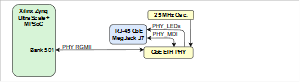 Image Added Image Added
|
|
8bit DACs
The TEC0850 Board has 4 8-bit parallel Texas Instruments THS5641AIPW digital to analog converter (DAC) with up to 100 MSPS update rate connected to TI THS4631D operational amplifiers. See Schematic circuitry and TI THS5641 data sheet for proper operation of the on-board DAC units.
| Scroll Title |
|---|
| anchor | Table_x |
|---|
| title | Table x: S2 DIP Switch |
|---|
|
| Scroll Table Layout |
|---|
| orientation | portrait |
|---|
| sortDirection | ASC |
|---|
| repeatTableHeaders | default |
|---|
| style | |
|---|
| widths | |
|---|
| sortByColumn | 1 |
|---|
| sortEnabled | false |
|---|
| cellHighlighting | true |
|---|
|
| DAC unit | Signal Schematic Name | Connected to | Functionality |
|---|
DAC1 U28 | DAC1_D0 | PL HD bank 50, pin D11 | Digital input bits D[7:0]
D7 is most significant data bit (MSB),
D0 is least significant data bit (LSB). | DAC1_D1 | PL HD bank 50, pin D10
| DAC1_D2 | PL HD bank 50, pin G11 | DAC1_D3 | PL HD bank 50, pin J11
| DAC1_D4 | PL HD bank 50, pin G10
| DAC1_D5 | PL HD bank 50, pin H10
| | DAC1_D6 | PL HD bank 50, pin J10 | | DAC1_D7 | PL HD bank 50, pin E10
| | DAC1_CLK | PL HD bank 50, pin F12 | External clock input, input data latched on rising edge of the clock. | | DAC1_MODE | PL HD bank 50, pin F10 | Input code format (binary, twos complement) | | EN_DAC1 | SC FPGA U18 bank 8, pinE6 | generate 3.3V voltages
LDO U35, U34 | DAC2 U31 | DAC2_D0 | PL HD bank 50, pin G15 | Digital input bits D[7:0]
D7 is most significant data bit (MSB),
D0 is least significant data bit (LSB). | DAC2_D1 | PL HD bank 50, pin H14
| DAC2_D2 | PL HD bank 50, pin J14
| | DAC2_D3 | PL HD bank 50, pin G14
| | DAC2_D4 | PL HD bank 50, pin G13
| | DAC2_D5 | PL HD bank 50, pin H13
| | DAC2_D6 | PL HD bank 50, pin H12 | | DAC2_D7 | PL HD bank 50, pin J12
| | DAC2_CLK | PL HD bank 50, pin F12
| External clock input, input data latched on rising edge of the clock. | | DAC2_MODE | PL HD bank 50, pin F11
| Input code format (binary, twos complement) | | EN_DAC2 | SC FPGA U18 bank 8, pin E8
| generate 3.3V voltages
LDO U32, U60 | DAC3 U29 | DAC3_D0 | PL HD bank 44, pin AG14
| Digital input bits D[7:0]
D7 is most significant data bit (MSB),
D0 is least significant data bit (LSB). | | DAC3_D1 | PL HD bank 44, pin AE13
| | DAC3_D2 | PL HD bank 44, pin AG13
| | DAC3_D3 | PL HD bank 44, pin AJ15
| | DAC3_D4 | PL HD bank 44, pin AJ14
| | DAC3_D5 | PL HD bank 44, pin AH14
| | DAC3_D6 | PL HD bank 44, pin AL13
| | DAC3_D7 | PL HD bank 44, pin AM13
| | DAC3_CLK | PL HD bank 44, pin AK15
| External clock input, input data latched on rising edge of the clock. | | DAC3_MODE | PL HD bank 44, pin AK14
| Input code format (binary, twos complement) | | EN_DAC3 | SC FPGA U18 bank 8, pin B6
| generate 3.3V voltages
LDO U66, U68 | DAC4 U33 | DAC4_D0 | PL HD bank 44, pin AP14
| Digital input bits D[7:0]
D7 is most significant data bit (MSB),
D0 is least significant data bit (LSB). | | DAC4_D1 | PL HD bank 44, pin AN14
| | DAC4_D2 | PL HD bank 44, pin AM14
| | DAC4_D3 | PL HD bank 44, pin AN13
| | DAC4_D4 | PL HD bank 44, pin AP12
| | DAC4_D5 | PL HD bank 44, pin AN12
| | DAC4_D6 | PL HD bank 44, pin AF13
| | DAC4_D7 | PL HD bank 44, pin AH13
| | DAC4_CLK | PL HD bank 44, pin AK13
| External clock input, input data latched on rising edge of the clock. | | DAC4_MODE | PL HD bank 44, pin AK13 | Input code format (binary, twos complement) | | EN_DAC4 | SC FPGA U18 bank 8, pin A6
| generate 3.3V voltages
LDO U70, U72 |
|
Gigabit Ethernet PHY
On-board Gigabit Ethernet PHY U20 is provided with Marvell Alaska 88E1512, which use MDIO address 1.. The Ethernet PHY RGMII interface is connected to the Zynq Ultrascale+ Ethernet0 PS GEM3. I/O voltage is fixed at 1.8V for HSTL signaling. The reference clock input of the PHY is supplied from the on-board 25.000000 MHz oscillator U21.
...
| anchor | Figure_11 |
|---|
| title | Figure 11: CAN interface |
|---|
...
| Scroll Only |
|---|
Image Removed |
8Bit DACs
Board has 4 8-bit parallel Texas Instruments THS5641 DACs with up to 100 MSPS Update Rate.
| Scroll Title |
|---|
| anchor | Figure_11 |
|---|
| title | Figure 11: CAN interface |
|---|
|
| Scroll Ignore |
|---|
scroll-only |
DIP-Switches
There are two 4-bit DIP-witches S3 and S4 present on the TEC0850 board to configure options and set parameters. The following section describes the functionalities of the particular switches.
...
| Scroll Title |
|---|
| anchor | Table_x |
|---|
| title | Table x: S2 DIP Switch |
|---|
|
| Scroll Table Layout |
|---|
| orientation | portrait |
|---|
| sortDirection | ASC |
|---|
| repeatTableHeaders | default |
|---|
| style | |
|---|
| widths | |
|---|
| sortByColumn | 1 |
|---|
| sortEnabled | false |
|---|
| cellHighlighting | true |
|---|
|
| DIP-switch S1 | Signal Schematic Name | Connected to | Functionality | Notes |
|---|
| S1-1 | JTAGEN | SC FPGA U18, bank 1B, pin E5 | Positions:
OFF: SC FPGA's JTAG enabled
ON: SC FPGA's JTAG disabled | switch the JTAG pins to user GPIO's if JTAG is disabled | | S1-2 | WP | EEPROM U63, pin 7 | Positions:
OFF: Write Protect is enabled
ON: Write Protect is disabled | - | | S1-3 | PUDC_B | Zynq MPSOC PS Config Bank 503, pin AD15 | Positions:
ON: PUDC_B is Low
OFF: PUDC_B is HIGH | Internal pull-up resistors during configuration
are enabled at ON-position,means I/O's are 3-stated
until configuration of the FPGA completes. | | S1-4 | SW4 | SC FPGA U18, bank 8, pin A5 | SC Switch (Reserved for future use) | low active logic | | DIP-switch S2 | Signal Schematic Name | Connected to | Functionality | Notes |
|---|
| S2-1 | MODE3 | Zynq MPSOC PS Config Bank 503, pin |
AD1511 : Boot Mode": ON | ON | ON | |
ON | JTAG Boot Mode
ON | ON | ON | |
OFF | OFF | SD Card | | S2-2 | MODE2 | Zynq MPSOC PS Config Bank 503, pin |
AD15T23 | | S2-3 | MODE1 | Zynq MPSOC PS Config Bank 503, pin |
AD15R22 | | S2-4 | MODE0 | Zynq MPSOC PS Config Bank 503, pin |
AD15 |
Buttons
There is one switch button available to the user connected to the SC FPGA U18:
...
| Include Page |
|---|
| IN:Legal Notices |
|---|
| IN:Legal Notices |
|---|
|