...
| Scroll Title |
|---|
| anchor | Figure_9 |
|---|
| title | Figure 9: 4x 8bit DAC units |
|---|
|
| Scroll Ignore |
|---|
| draw.io Diagram |
|---|
| border | false |
|---|
| viewerToolbar | true |
|---|
| |
|---|
| fitWindow | false |
|---|
| diagramDisplayName | |
|---|
| lbox | true |
|---|
| revision | 3 |
|---|
| diagramName | TEC0850 DACs |
|---|
| simpleViewer | false |
|---|
| width | |
|---|
| links | auto |
|---|
| tbstyle | hidden |
|---|
| diagramWidth | 641 |
|---|
|
|
| Scroll Only |
|---|
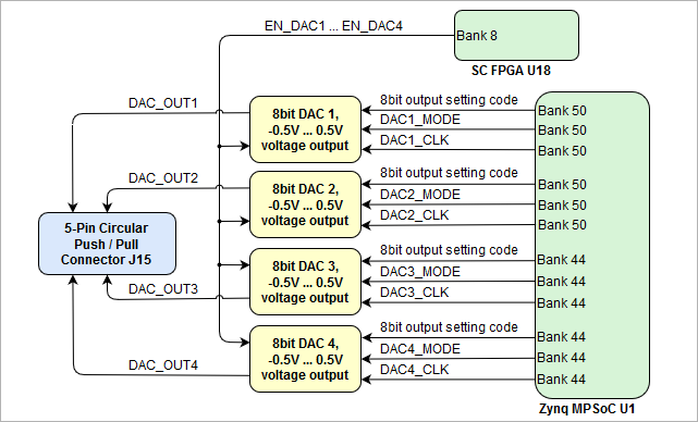 Image Added Image Added
|
|
There is a 26-pin IDC header (2x13, 1.27mm grid size) J16 available on the TEC0850 board which exposes the 20 FPGA HD I/O's of PL bank 47 to the user. The PL bank 47 has 3.3V VCCO bank voltage, on the header J16 there also the voltage levels 3.3V and 5V available. The I/O's can be accessed with a corresponding IDC connector.
| Scroll Title |
|---|
| anchor | Figure_10 |
|---|
| title | Figure 10: Zynq MPSoC PL I/O's IDC pin-header |
|---|
|
| Scroll Ignore |
|---|
| draw.io Diagram |
|---|
| border | false |
|---|
| viewerToolbar | true |
|---|
| |
|---|
| fitWindow | false |
|---|
| diagramDisplayName | |
|---|
| lbox | true |
|---|
| revision | 3 |
|---|
| diagramName | TEC0850 header J16 |
|---|
| simpleViewer | false |
|---|
| width | |
|---|
| links | auto |
|---|
| tbstyle | hidden |
|---|
| diagramWidth | 641 |
|---|
|
|
| Scroll Only |
|---|
 Image Added Image Added
|
|
On the TEC0850 there is a 10-pin SMT header (2x5, 2.54mm grid size) J13 present which provides access to the JTAG and UART interface of Altera MAX10 System Controller FPGA. The header J13 has a compatible pin assignment to the TEI0004 JTAG programmer for Altera FPGAs, the voltage levels 3.3V is on the header available as reference I/O-voltage for JTAG and UART.
...
| Scroll Title |
|---|
| anchor | Figure_11 |
|---|
| title | Figure 11: 10-pin JTAG/UART header |
|---|
|
| Scroll Ignore |
|---|
| draw.io Diagram |
|---|
| border | false |
|---|
| viewerToolbar | true |
|---|
| |
|---|
| fitWindow | false |
|---|
| diagramDisplayName | |
|---|
| lbox | true |
|---|
| revision | 3 |
|---|
| diagramName | TEC0850 header 13 |
|---|
| simpleViewer | false |
|---|
| width | |
|---|
| links | auto |
|---|
| tbstyle | hidden |
|---|
| diagramWidth | 641 |
|---|
|
|
| Scroll Only |
|---|
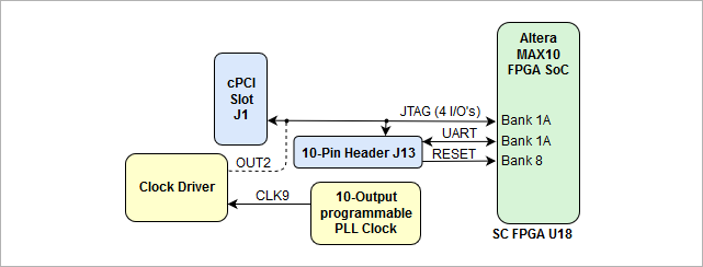 Image Added Image Added
|
|
2 I/O's of the SC FPGA U18 are exposed to the on-board 3-Pin PicoBlade header J8 available to the user or for future use of upcoming versions of SC FPGA firmware.
| Scroll Title |
|---|
| anchor | Figure_12 |
|---|
| title | Figure 12: 3-pin PicoBlade header |
|---|
|
| Scroll Ignore |
|---|
| draw.io Diagram |
|---|
| border | false |
|---|
| viewerToolbar | true |
|---|
| |
|---|
| fitWindow | false |
|---|
| diagramDisplayName | |
|---|
| lbox | true |
|---|
| revision | 1 |
|---|
| diagramName | TEC0850 3-pin header J8 |
|---|
| simpleViewer | false |
|---|
| width | |
|---|
| links | auto |
|---|
| tbstyle | hidden |
|---|
| diagramWidth | 641 |
|---|
|
|
| Scroll Only |
|---|
 Image Added Image Added
|
|
Battery Holder
There is a CR1220 battery holder available to the supply the voltage for the for for the Zynq MPSoC's Battery Power Domain (BBRAM and RTC). The battery voltage VBATT should be in the range of 2.2V to 5.5V, use 3.0V CR1220 battery.
| Scroll Title |
|---|
| anchor | Figure_13 |
|---|
| title | Figure 13: Backup-Battery Holder |
|---|
|
| Scroll Ignore |
|---|
| draw.io Diagram |
|---|
| border | false |
|---|
| viewerToolbar | true |
|---|
| |
|---|
| fitWindow | false |
|---|
| diagramDisplayName | |
|---|
| lbox | true |
|---|
| revision | 4 |
|---|
| diagramName | TEC0850 battery holder |
|---|
| simpleViewer | false |
|---|
| width | |
|---|
| links | auto |
|---|
| tbstyle | hidden |
|---|
| diagramWidth | 641 |
|---|
|
|
| Scroll Only |
|---|
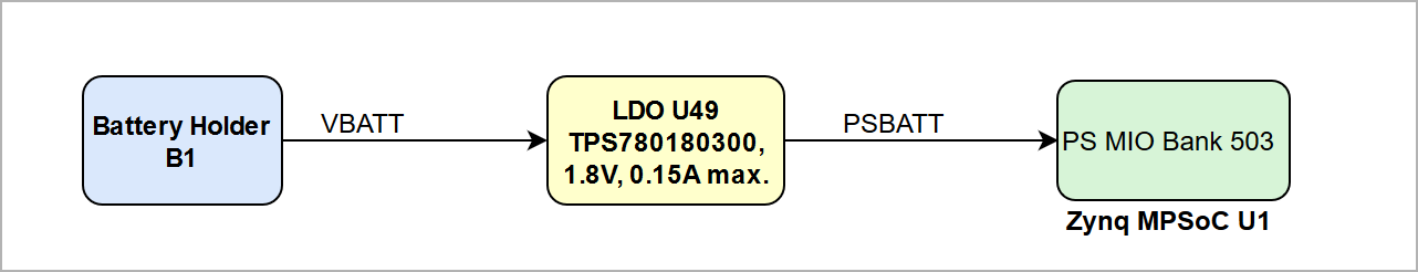 Image Added Image Added
|
|
4-Wire PWM FAN Connectors
...
| Scroll Title |
|---|
| anchor | Figure_15 |
|---|
| title | Figure 15: TEC0850 MAX10 System Controller FPGA |
|---|
|
| Scroll Ignore |
|---|
| draw.io Diagram |
|---|
| border | false |
|---|
| viewerToolbar | true |
|---|
| |
|---|
| fitWindow | false |
|---|
| diagramDisplayName | |
|---|
| lbox | true |
|---|
| revision | 2 |
|---|
| diagramName | TEC0850 SC TO Zynq connections |
|---|
| simpleViewer | false |
|---|
| width | |
|---|
| links | auto |
|---|
| tbstyle | hidden |
|---|
| diagramWidth | 641 |
|---|
|
|
| Scroll Only |
|---|
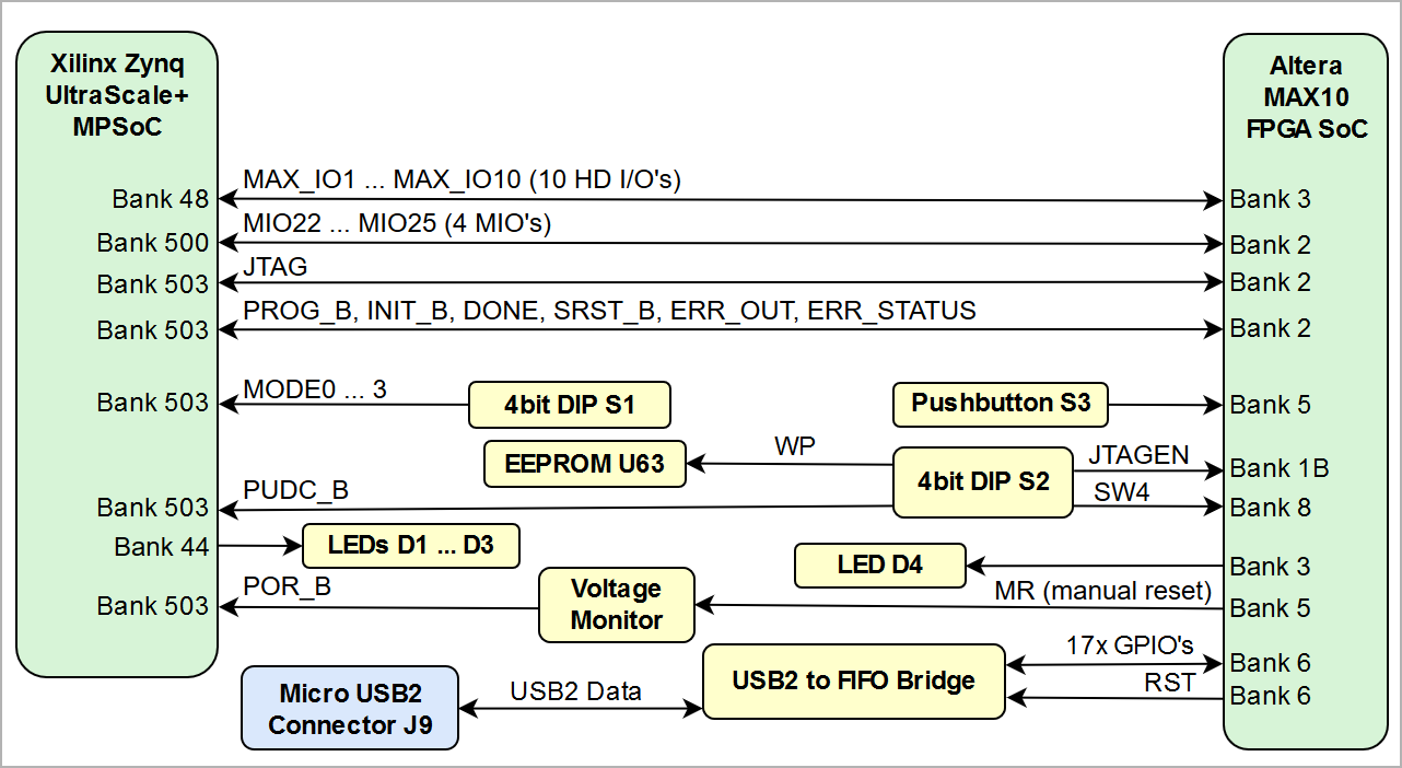 Image Added Image Added
|
|
Programmable Clock Generator
...
| Scroll Title |
|---|
| anchor | Figure_16 |
|---|
| title | Figure 16: 10-output I²C programmable clock generator |
|---|
|
| Scroll Ignore |
|---|
| draw.io Diagram |
|---|
| border | false |
|---|
| viewerToolbar | true |
|---|
| |
|---|
| fitWindow | false |
|---|
| diagramDisplayName | |
|---|
| lbox | true |
|---|
| revision | 4 |
|---|
| diagramName | TEC0850 clock sourdes |
|---|
| simpleViewer | false |
|---|
| width | |
|---|
| links | auto |
|---|
| tbstyle | hidden |
|---|
| diagramWidth | 641 |
|---|
|
|
| Scroll Only |
|---|
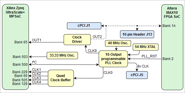 Image Added Image Added
|
|
Following table shows on-board Silicon Labs I2C programmable Si5345A U17 10-output programmable PLL reference clock generator inputs and outputs:
...
| Scroll Title |
|---|
| anchor | Figure_17 |
|---|
| title | Figure 17: TEC0850 on-board FTDI chips |
|---|
|
| Scroll Ignore |
|---|
| draw.io Diagram |
|---|
| border | false |
|---|
| viewerToolbar | true |
|---|
| |
|---|
| fitWindow | false |
|---|
| diagramDisplayName | |
|---|
| lbox | true |
|---|
| revision | 4 |
|---|
| diagramName | TEC0850 FT2232H |
|---|
| simpleViewer | false |
|---|
| width | |
|---|
| links | auto |
|---|
| tbstyle | hidden |
|---|
| diagramWidth | 641 |
|---|
|
|
| Scroll Only |
|---|
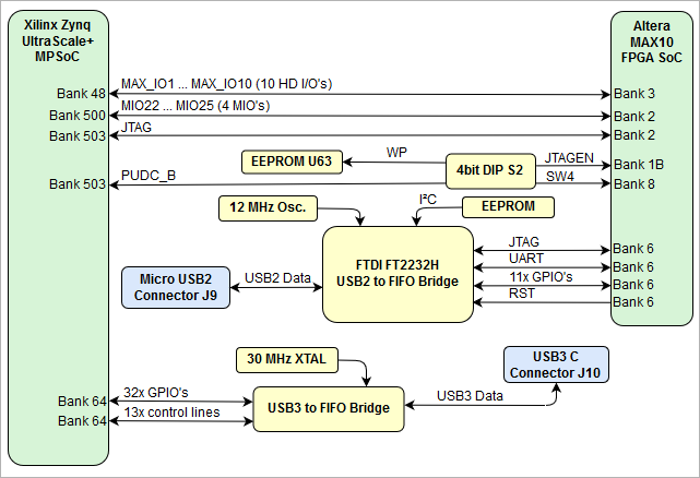 Image Added Image Added
|
|
FT2232H
The TEC0850 board is equipped with the FTDI FT2232H USB2 to JTAG/UART adapter controller connected to micro-USB2 connector J9 to provide JTAG and UART access to the Xilinx Zynq XC7Z010 SoC. There is also a 256-byte configuration EEPROM U6 wired to the FT2232H chip via Microwire bus which holds pre-programmed license code to support Xilinx programming tools. Refer to the FTDI data sheet to get information about the capacity of the FT2232H chip.
...
| Scroll Title |
|---|
| anchor | Figure_18 |
|---|
| title | Figure 18: Quad-SPI Flash Memory |
|---|
|
| Scroll Ignore |
|---|
| draw.io Diagram |
|---|
| border | false |
|---|
| viewerToolbar | true |
|---|
| |
|---|
| fitWindow | false |
|---|
| diagramDisplayName | |
|---|
| lbox | true |
|---|
| revision | 1 |
|---|
| diagramName | TEC0850 QSPI Flash |
|---|
| simpleViewer | false |
|---|
| width | |
|---|
| links | auto |
|---|
| tbstyle | hidden |
|---|
| diagramWidth | 641 |
|---|
|
|
| Scroll Only |
|---|
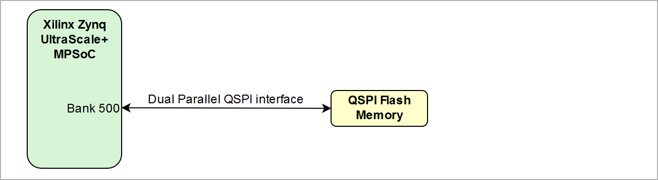 Image Added Image Added
|
|
| Scroll Title |
|---|
| anchor | Table_20 |
|---|
| title | Table 20: Quad-SPI Flash memory interface connections |
|---|
|
| Scroll Table Layout |
|---|
| orientation | portrait |
|---|
| sortDirection | ASC |
|---|
| repeatTableHeaders | default |
|---|
| style | |
|---|
| widths | |
|---|
| sortByColumn | 1 |
|---|
| sortEnabled | false |
|---|
| cellHighlighting | true |
|---|
|
| IC | Memory Density | MIO | Signal Schematic Name | Flash Memory Pin |
|---|
QSPI Flash U24, N25Q256A11E1240E | 256 Mbit (32 MByte) | 0 | MIO0 | B2 | | 1 | MIO1 | D2 | | 2 | MIO2 | C4 | | 3 | MIO3 | D4 | | 4 | MIO4 | D3 | | 5 | MIO5 | C2 | QSPI Flash U25, N25Q256A11E1240 | 256 Mbit (32 MByte) | 7 | MIO7 | C2 | | 8 | MIO8 | D3 | | 9 | MIO9 | D2 | | 10 | MIO10 | C4 | | 11 | MIO11 | D4 | | 12 | MIO12 | B2 |
|
...
| Scroll Title |
|---|
| anchor | Figure_19 |
|---|
| title | Figure 19: On-board configuration EEPROMs |
|---|
|
| Scroll Ignore |
|---|
| draw.io Diagram |
|---|
| border | false |
|---|
| viewerToolbar | true |
|---|
| |
|---|
| fitWindow | false |
|---|
| diagramDisplayName | |
|---|
| lbox | true |
|---|
| revision | 2 |
|---|
| diagramName | TEC0850 USB3 to FIFO |
|---|
| simpleViewer | false |
|---|
| width | |
|---|
| links | auto |
|---|
| tbstyle | hidden |
|---|
| diagramWidth | 641 |
|---|
|
|
| Scroll Only |
|---|
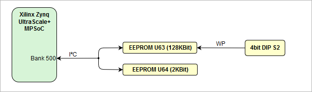 Image Added Image Added
|
|
The EEPROMs U63 and U64 are programmable via the on-board I²C bus connected to MIO 20...21 pins. The I²C address is shown in the table below.
...
| Scroll Title |
|---|
| anchor | Figure_20 |
|---|
| title | Figure 20: TEC0850 cPCI USB2 interface |
|---|
|
| Scroll Ignore |
|---|
| draw.io Diagram |
|---|
| border | false |
|---|
| viewerToolbar | true |
|---|
| |
|---|
| fitWindow | false |
|---|
| diagramDisplayName | |
|---|
| lbox | true |
|---|
| revision | 1 |
|---|
| diagramName | TEC0850 USB2 PHY |
|---|
| simpleViewer | false |
|---|
| width | |
|---|
| links | auto |
|---|
| tbstyle | hidden |
|---|
| diagramWidth | 641 |
|---|
|
|
| Scroll Only |
|---|
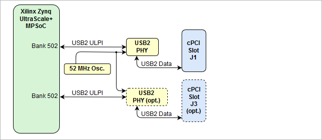 Image Added Image Added
|
|
| Scroll Title |
|---|
| anchor | Table_22 |
|---|
| title | Table 22: USB2 ULPI interface description |
|---|
|
| Scroll Table Layout |
|---|
| orientation | portrait |
|---|
| sortDirection | ASC |
|---|
| repeatTableHeaders | default |
|---|
| style | |
|---|
| widths | |
|---|
| sortByColumn | 1 |
|---|
| sortEnabled | false |
|---|
| cellHighlighting | true |
|---|
|
| PHY Pin | Connected to | Notes |
|---|
| ULPI | PS bank MIO52 ... MIO63 | Zynq Ultrascale+ USB0 MIO pins are connected to the PHY | | REFCLK | - | 52MHz from on board oscillator U12 | | REFSEL[0..2] | - | All pins set to GND selects the external reference clock frequency (52.000000 MHz) | | RESETB | Zynq MPSoC MIO16, pin AM16 | Low active USB2 PHY Reset
| | DP, DM | cPCI connector J1 | USB2 data lane | | CPEN | - | External USB power switch active-high enable signal | | VBUS | 5V | Connected to USB VBUS via a series of resistors, see schematic | | ID | 3.3V | B-device |
|
...