...
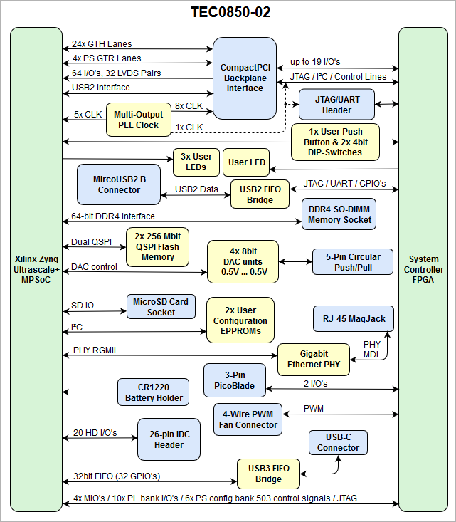
| Scroll Title |
|---|
| anchor | Figure_BD |
|---|
| title | Figure 1: TEC0850-02 block diagram |
|---|
|
| Scroll Ignore |
|---|
| draw.io Diagram |
|---|
| border | false |
|---|
| viewerToolbar | true |
|---|
| |
|---|
| fitWindow | false |
|---|
| diagramDisplayName | |
|---|
| lbox | true |
|---|
| revision | 56 |
|---|
| diagramName | TEC0850 overview |
|---|
| simpleViewer | false |
|---|
| width | |
|---|
| links | auto |
|---|
| tbstyle | hidden |
|---|
| diagramWidth | 641 |
|---|
|
|
| Scroll Only |
|---|
|
|
...
| Scroll Title |
|---|
| anchor | Figure_CompactPCI |
|---|
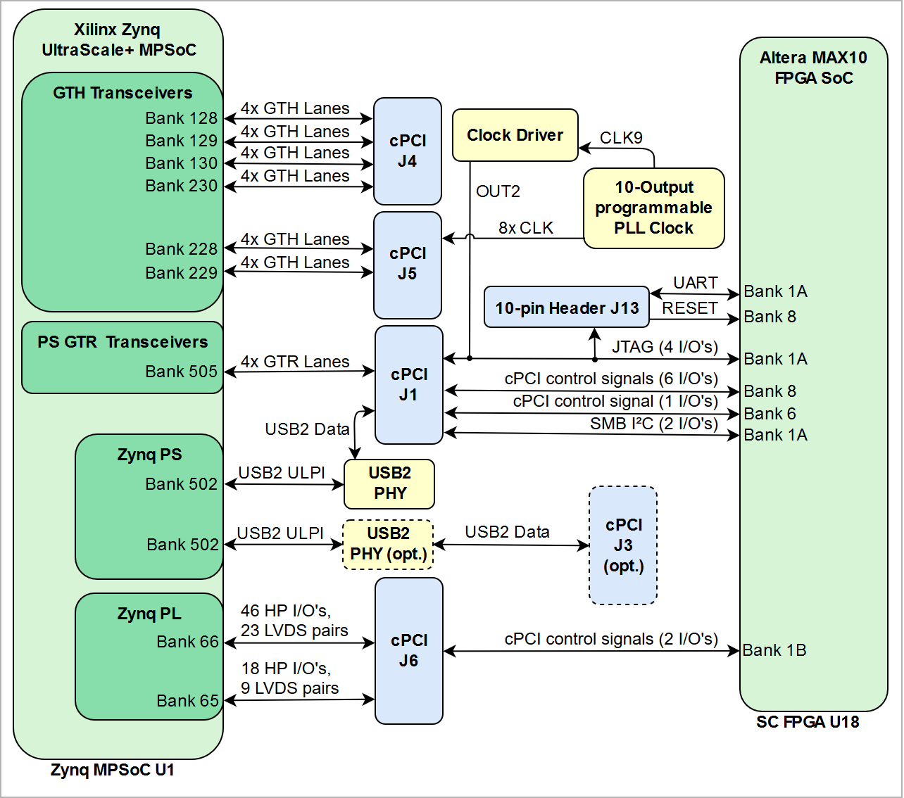
| title | Figure 3: TEC0850-02 CompactPCI I/O and high-speed interfaces |
|---|
|
| Scroll Ignore |
|---|
| draw.io Diagram |
|---|
| border | false |
|---|
| viewerToolbar | true |
|---|
| |
|---|
| fitWindow | false |
|---|
| diagramDisplayName | |
|---|
| lbox | true |
|---|
| revision | 1718 |
|---|
| diagramName | IO Diagram |
|---|
| simpleViewer | false |
|---|
| width | |
|---|
| links | auto |
|---|
| tbstyle | hidden |
|---|
| diagramWidth | 641642 |
|---|
|
|
| Scroll Only |
|---|
|
|
Following tables contains information about the interfaces, I/O's, clock and VCCIO sources available on the cPCI connectors:
- CompactPCI Connector J1
- Optional CompactPCI Connector J2
- CompactPCI Connector J4
- CompactPCI Connector J5
- CompactPCI Connector J6
...
| Scroll Title |
|---|
| anchor | Table_cPCI_J1_sata |
|---|
| title | Table 5: cPCI J1 clock signals |
|---|
|
| Scroll Table Layout |
|---|
| orientation | portrait |
|---|
| sortDirection | ASC |
|---|
| repeatTableHeaders | default |
|---|
| style | |
|---|
| widths | |
|---|
| sortByColumn | 1 |
|---|
| sortEnabled | false |
|---|
| cellHighlighting | true |
|---|
|
| Clock Signal Schematic Name | cPCI Connector Pin | Header J13 Pin | SC FPGA U18 Pin | Notes |
|---|
| J1-K3
J1-J3 | J13-5
J13-1 | Bank 1B, Pin G1
Bank 1B, Pin G2 | Supplied by 10-output PLL clock U14,
optional if decoupling capacitors and resistors
are fitted (see schematic),cPCI connector J1 clock signal from PLL U14 is
also shared with SC FPGA and header J13. |
|
| Anchor |
|---|
| CompactPCI Connector J2 |
|---|
| CompactPCI Connector J2 |
|---|
|
Optional CompactPCI Connector J2
CompactPCI connector J2 is not fitted on the TEC0850 board by default, but is necessary if the second optional USB2 PHY U13 if fitted and its USB2 differential serial data interface is connected to the cPCI connector J2.
| Anchor |
|---|
| CompactPCI Connector J4 |
|---|
| CompactPCI Connector J4 |
|---|
|
CompactPCI Connector J4
| Scroll Title |
|---|
| anchor | Table_cPCI_J4_mgt |
|---|
| title | Table 6: cPCI J4 MGT lanes |
|---|
|
| Scroll Table Layout |
|---|
| orientation | portrait |
|---|
| sortDirection | ASC |
|---|
| repeatTableHeaders | default |
|---|
| style | |
|---|
| widths | |
|---|
| sortByColumn | 1 |
|---|
| sortEnabled | false |
|---|
| cellHighlighting | true |
|---|
|
| MGT Lane | Bank | Type | Signal Schematic Name | cPCI Connector Pin | FPGA Pin |
|---|
| 0 | 128 | GTH | - PE3_RX0_P
- PE3_RX0_N
- PE3_TX0_P
- PE3_TX0_N
| J4-D1
J4-E1
J4-A1
J4-B1 | MGTHRXP0_128, T33
MGTHRXN0_128, T34
MGTHTXP0_128, T29
MGTHTXN0_128, T30 | | 1 | 128 | GTH | - PE3_RX1_P
- PE3_RX1_N
- PE3_TX1_P
- PE3_TX1_N
| J4-J1
J4-K1
J4-G1
J4-H1 | MGTHRXP1_128, P33
MGTHRXN1_128, P34
MGTHTXP1_128, R31
MGTHTXN1_128, R32 | | 2 | 128 | GTH | - PE3_RX2_P
- PE3_RX2_N
- PE3_TX2_P
- PE3_TX2_N
| J4-E2
J4-F2
J4-B2
J4-C2 | MGTHRXP2_128, N31
MGTHRXN2_128, N32
MGTHTXP2_128, P29
MGTHTXN2_128, P30 | | 3 | 128 | GTH | - PE3_RX3_P
- PE3_RX3_N
- PE3_TX3_P
- PE3_TX3_N
| J4-K2
J4-L2
J4-H2
J4-I2 | MGTHRXP3_128, M33
MGTHRXN3_128, M34
MGTHTXP3_128, M29
MGTHTXN3_128, M30 | | 0 | 129 | GTH | - PE4_RX0_P
- PE4_RX0_N
- PE4_TX0_P
- PE4_TX0_N
| J4-D3
J4-E3
J4-A3
J4-B3 | MGTHRXP0_129, L31
MGTHRXN0_129, L32
MGTHTXP0_129, K29
MGTHTXN0_129, K30 | | 1 | 129 | GTH | - PE4_RX1_P
- PE4_RX1_N
- PE4_TX1_P
- PE4_TX1_N
| J4-J3
J4-K3
J4-G3
J4-H3 | MGTHRXP1_129, K33
MGTHRXN1_129, K34
MGTHTXP1_129, J31
MGTHTXN1_129, J32 | | 2 | 129 | GTH | - PE4_RX2_P
- PE4_RX2_N
- PE4_TX2_P
- PE4_TX2_N
| J4-E4
J4-F4
J4-B4
J4-C4 | MGTHRXP2_129, H33
MGTHRXN2_129, H34
MGTHTXP2_129, H29
MGTHTXN2_129, H30 | | 3 | 129 | GTH | - PE4_RX3_P
- PE4_RX3_N
- PE4_TX3_P
- PE4_TX3_N
| J4-K4
J4-L4
J4-H4
J4-I4 | MGTHRXP3_129, F33
MGTHRXN3_129, F34
MGTHTXP3_129, G31
MGTHTXN3_129, G32 | | 0 | 130 | GTH | - PE5_RX0_P
- PE5_RX0_N
- PE5_TX0_P
- PE5_TX0_N
| J4-D5
J4-E5
J4-A5
J4-B5 | MGTHRXP3_130, B33
MGTHRXN3_130, B34
MGTHTXP3_130, A31
MGTHTXN3_130, A32 | | 1 | 130 | GTH | - PE5_RX1_P
- PE5_RX1_N
- PE5_TX1_P
- PE5_TX1_N
| J4-J5
J4-K5
J4-G5
J4-H5 | MGTHRXP2_130, C31
MGTHRXN2_130, C32
MGTHTXP2_130, B29
MGTHTXN2_130, B30 | | 2 | 130 | GTH | - PE5_RX2_P
- PE5_RX2_N
- PE5_TX2_P
- PE5_TX2_N
| J4-E6
J4-F6
J4-B6
J4-C6 | MGTHRXP1_130, D33
MGTHRXN1_130, D34
MGTHTXP1_130, D29
MGTHTXN1_130, D30 | | 3 | 130 | GTH | - PE5_RX3_P
- PE5_RX3_N
- PE5_TX3_P
- PE5_TX3_N
| J4-K6
J4-L6
J4-H6
J4-I6 | MGTHRXP0_130, E31
MGTHRXN0_130, E32
MGTHTXP0_130, F29
MGTHTXN0_130, F30 | | 0 | 230 | GTH | - PE6_RX0_P
- PE6_RX0_N
- PE6_TX0_P
- PE6_TX0_N
| J4-D7
J4-E7
J4-A7
J4-B7 | MGTHRXP3_230, A4
MGTHRXN3_230, A3
MGTHTXP3_230, A8
MGTHTXN3_230, A7 | | 1 | 230 | GTH | - PE6_RX1_P
- PE6_RX1_N
- PE6_TX1_P
- PE6_TX1_N
| J4-J7
J4-K7
J4-G7
J4-H7 | MGTHRXP2_230, B2
MGTHRXN2_230, B1
MGTHTXP2_230, B6
MGTHTXN2_230, B5 | | 2 | 230 | GTH | - PE6_RX2_P
- PE6_RX2_N
- PE6_TX2_P
- PE6_TX2_N
| J4-E8
J4-F8
J4-B8
J4-C8 | MGTHRXP1_230, C4
MGTHRXN1_230, C3
MGTHTXP1_230, D6
MGTHTXN1_230, D5 | | 3 | 230 | GTH | - PE6_RX3_P
- PE6_RX3_N
- PE6_TX3_P
- PE6_TX3_N
| J4-K8
J4-L8
J4-H8
J4-I8 | MGTHRXP0_230, D2
MGTHRXN0_230, D1
MGTHTXP0_230, E4
MGTHTXN0_230, E3 |
|
...
| Scroll Title |
|---|
| anchor | Figure_si5345 |
|---|
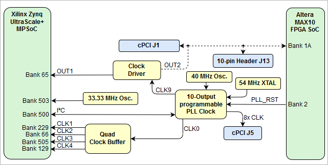
| title | Figure 16: 10-output I²C programmable clock generator |
|---|
|
| Scroll Ignore |
|---|
| draw.io Diagram |
|---|
| border | false |
|---|
| viewerToolbar | true |
|---|
| |
|---|
| fitWindow | false |
|---|
| diagramDisplayName | |
|---|
| lbox | true |
|---|
| revision | 45 |
|---|
| diagramName | TEC0850 clock sourdes |
|---|
| simpleViewer | false |
|---|
| width | |
|---|
| links | auto |
|---|
| tbstyle | hidden |
|---|
| diagramWidth | 641 |
|---|
|
|
| Scroll Only |
|---|
|
|
...
| Scroll Title |
|---|
| anchor | Table_si5345 |
|---|
| title | Table 14: SI5345 Clock Outputs |
|---|
|
| Scroll Table Layout |
|---|
| orientation | portrait |
|---|
| sortDirection | ASC |
|---|
| repeatTableHeaders | default |
|---|
| style | |
|---|
| widths | |
|---|
| sortByColumn | 1 |
|---|
| sortEnabled | false |
|---|
| cellHighlighting | true |
|---|
|
Si5345A U14 Pin
| Signal Schematic Name
| Connected to | Clock Signal Direction | Note |
|---|
| IN0 | | 40.000 MHz Oscillator U75 | Input | external reference
clock input | | GND | | IN1 | - | not connected | Input | not used | | - | not connected | | IN2 | - | not connected | Input | not used | | - | not connected | | IN3 | - | not connected | Input | not used
| | - | not connected | | OUT0 | | Quad clock buffer
Si53340 U16 | Output | reference clock input to
Quad clock buffer | | | OUT1 | | cPCI J5, pin B5 | Output | reference clock output
to cPCI connector J5 | | cPCI J5, pin A5 | | OUT2 | | cPCI J5, pin C6 | Output | | cPCI J5, pin B6 | | OUT3 | | cPCI J5, pin E5 | Output | | cPCI J5, pin D5 | | OUT4 | | cPCI J5, pin H5 | Output | | cPCI J5, pin G5 | | OUT5 | | cPCI J5, pin K5 | Output | | cPCI J5, pin J5 | | OUT6 | | cPCI J5, pin F6 | Output | | cPCI J5, pin E6 | | OUT7 | | cPCI J5, pin L6 | Output | | cPCI J5, pin K6 | | OUT8 | | cPCI J5, pin I6 | Output | | cPCI J5, pin H6 | | OUT9 | | Clock Driver LTC6975 U73 | Output | reference clock input to
dual clock driver U73 | | | XA/XB | | 54.000 MHz quartz
oscillator Y3 | Input | Differential quartz oscillator
clock input | | SCLK,
SDA/SDIO | | | BiDir | I²C address 0x69 |
|
...
| Scroll Title |
|---|
| anchor | Table_clk_buffer |
|---|
| title | Table 15: Clock driver and buffer outputs |
|---|
|
| Scroll Table Layout |
|---|
| orientation | portrait |
|---|
| sortDirection | ASC |
|---|
| repeatTableHeaders | default |
|---|
| style | |
|---|
| widths | |
|---|
| sortByColumn | 1 |
|---|
| sortEnabled | false |
|---|
| cellHighlighting | true |
|---|
|
Si53340 U16 Pin
| Signal Schematic Name
| Connected to | Clock Signal Direction | Note |
|---|
| Q0 | | U1, pin G8
U1, pin G7 | Output | GTH bank 229 reference clock input | | Q1 | | U1, pin Y8
U1, pin Y7 | Output | PL HP bank 66 reference clock input | | Q2 | | U1, pin U27
U1, pin U28 | Output | PS GTR Bank 505 reference clock input | | Q3 | | U1, pin L27
U1, pin L28 | Output | GTH bank 129 reference clock input | | LTC6957 U14 U73 Pin |
|
|
|
|
|---|
| OUT1 | | U1, pin AG5
U1, pin AG4 | Output | PL HP bank 65 reference clock input | | OUT2 | | Signal 'SATA_SL'
Signal 'SATA_SCL' | Output | optional reference clock input to cPCI connector J1,
header J13 and SC FPGA U18 if decoupling capacitors and resistors
are fitted (see schematic),
also shared with SC FPGA and header J13 |
|
The clock generator U14 is programmable via the onboard I²C bus connected to MIO 20...21 pins. The I²C address is shown in the table below.
...
| Scroll Title |
|---|
| anchor | Table_usb2_phy_io |
|---|
| title | Table 22: USB2 ULPI interface description |
|---|
|
| Scroll Table Layout |
|---|
| orientation | portrait |
|---|
| sortDirection | ASC |
|---|
| repeatTableHeaders | default |
|---|
| style | |
|---|
| widths | |
|---|
| sortByColumn | 1 |
|---|
| sortEnabled | false |
|---|
| cellHighlighting | true |
|---|
|
| USB2 PHY U11 Pin | Connected to | Notes |
|---|
| ULPI | PS bank MIO52 ... MIO63 | Zynq Ultrascale+ USB0 MIO pins are connected to the PHY | | REFCLK | - | 52MHz from onboard oscillator U12 | | REFSEL[0..2] | - | All pins set to GND selects the external reference clock frequency (52.000000 MHz) | | RESETB | Zynq MPSoC MIO16, pin AM16 | Low active USB2 PHY Reset
| | DP, DM | cPCI connector J1 | USB2 data lane | | CPEN | - | External USB power switch active-high enable signal | | VBUS | 5V | Connected to onboard 5V voltage level via a series of resistors, see schematic | | ID | 3.3V | B-deviceUSB2 OTG A-Device (host) | | optional USB2 PHY U13 Pin | Connected to | Notes |
|---|
| ULPI | PS bank MIO64 ... MIO75 | Zynq Ultrascale+ USB1 MIO pins are connected to the PHY | | REFCLK | - | 52MHz from onboard oscillator U12 | | REFSEL[0..2] | - | All pins set to GND selects the external reference clock frequency (52.000000 MHz) | | RESETB | Zynq MPSoC MIO17, pin AP16 | Low active USB2 PHY Reset | | DP, DM | optional cPCI connector J3 | USB2 data lane | | CPEN | - | External USB power switch active-high enable signal | | VBUS | 5V | Connected to onboard 5V voltage level via a series of resistors, see schematic | | ID | 3.3V | B-deviceUSB2 OTG A-Device (host) |
|
Gigabit Ethernet PHY
Onboard Gigabit Ethernet PHY U20 is provided with Marvell Alaska 88E1512, which use MDIO address 1. The Ethernet PHY RGMII interface is connected to the Zynq Ultrascale+ Ethernet0 PS GEM3. I/O voltage is fixed at 1.8V for HSTL signaling. The reference clock input of the PHY is supplied from the on-board 25.000000 MHz oscillator U21.
...
| Scroll Title |
|---|
| anchor | Table_Document_Change_History |
|---|
| title | Table 34: Document change history |
|---|
|
| Scroll Table Layout |
|---|
| orientation | portrait |
|---|
| sortDirection | ASC |
|---|
| repeatTableHeaders | default |
|---|
| style | |
|---|
| widths | |
|---|
| sortByColumn | 1 |
|---|
| sortEnabled | false |
|---|
| cellHighlighting | true |
|---|
|
| Date | Revision | Constributor | Description |
|---|
| Page info |
|---|
| infoType | Modified date |
|---|
| dateFormat | yyyy-MM-dd |
|---|
| type | Flat |
|---|
|
| | Page info |
|---|
| infoType | Current version |
|---|
| prefix | v. |
|---|
| type | Flat |
|---|
| showVersions | false |
|---|
|
| | Page info |
|---|
| infoType | Modified by |
|---|
| type | Flat |
|---|
| showVersions | false |
|---|
|
| - added information about the optional
second USB2 PHY and cPCI connector J2
(not fitted by default)
| 2018-09-19 | | | | | v.93 | Ali Naseri , Oleksandr Kiyenko , John Hartfiel | | | -- | all | | Page info |
|---|
| infoType | Modified users |
|---|
| type | Flat |
|---|
| showVersions | false |
|---|
|
| |
|
...
| Include Page |
|---|
| IN:Legal Notices |
|---|
| IN:Legal Notices |
|---|
|
John Hartfiel